TBU-CX050-VTC-WH Bourns Inc., TBU-CX050-VTC-WH Datasheet
TBU-CX050-VTC-WH
Specifications of TBU-CX050-VTC-WH


Related parts for TBU-CX050-VTC-WH

TBU-CX050-VTC-WH Summary of contents
Page 1
... TBU-CX050-VTC-WH TBU-CX065-VTC-WH TBU-CX085-VTC-WH Part Number TBU-CXxxx-VTC-WH = 250 V I (min.) = 500 mA TBU-CX025-VTC-WH trigger = 400 V I (min.) = 500 mA TBU-CX040-VTC-WH trigger = 500 V I (min.) = 500 mA TBU-CX050-VTC-WH trigger = 650 V I (min.) = 500 mA TBU-CX065-VTC-WH trigger = 850 V I (min.) = 500 mA TBU-CX085-VTC-WH trigger Applications ■ Voice / VDSL cards ■ ...
Page 2
... Device Equip. TBU ® Device R Performance Graphs Typical V-I Characteristics (TBU-CX050-VTC-WH with Rext = 1 Ω) CURRENT (100 mA/div) High-Speed Protectors Basic TBU Operation The TBU technology, placed in the system circuit will monitor the current with the MOSFET detection circuit triggering to provide an effective barrier behind which sensitive electronics are not exposed to large voltages or currents during surge events ...
Page 3
... TBU-CX Series - TBU Performance Graphs (Continued) Power Derating Curve 3.0 No Additional PCB Cu 0.5 sq. in. Additional PCB Cu 2.5 2.0 1.5 1.0 0.5 0 100 Ambient Temperature (°C) Typical Resistance vs. Temperature 2.2 2.0 1.8 1.6 1.4 1.2 1.0 0.8 0.6 0.4 0.2 0.0 ...
Page 4
... TBU-CX Series - TBU Recommended Pad Layout TBU ® protectors have matte-tin termination fi nish. The suggested layout should use Non-Solder Mask Defi ne (NSMD). The recommended stencil thickness is 0.10-0.12 mm (.004- .005 in.) with a stencil opening size 0.025 mm (.0010 in.) less than the device pad size. As when heat sinking any power device recommended that wherever possible, extra PCB copper area is allowed ...
Page 5
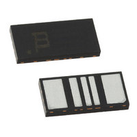
... REV. 04/11 “TBU” registered trademark of Bourns, Inc. in the U.S., Taiwan and European Community. Specifi cations are subject to change without notice. Customers should verify actual device performance in their specifi c applications. ® High-Speed Protectors Typical Part Marking ...