TCST2103 Vishay, TCST2103 Datasheet - Page 3
TCST2103
Manufacturer Part Number
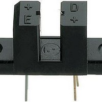
TCST2103
Description
SENSR OPTO SLOT 3.1MM TRANS THRU
Manufacturer
Vishay
Type
Unamplifiedr
Datasheet
1.TCST2103.pdf
(7 pages)
Specifications of TCST2103
Sensing Distance
3.1mm
Sensing Method
Transmissive
Output Configuration
Phototransistor
Current - Dc Forward (if)
60mA
Current - Collector (ic) (max)
4mA
Voltage - Collector Emitter Breakdown (max)
70V
Response Time
10µs, 8µs
Mounting Type
Through Hole
Package / Case
Slotted Module, 4-Lead Dual Row
Operating Temperature
-55°C ~ 85°C
Maximum Operating Temperature
+ 85 C
Minimum Operating Temperature
- 55 C
Wavelength
950 nm
Output Collector Emitter Voltage (detector)
70 V
Maximum Reverse Voltage (emitter)
6 V
Maximum Collector Current (detector)
100 mA
Slot Width
3.1 mm
Aperture Width
1 mm
Output Device
Phototransistor
Power Dissipation
250 mW
No. Of Channels
1
Optocoupler Output Type
Phototransistor
Input Current
60mA
Output Voltage
70V
Opto Case Style
Through Hole
No. Of Pins
4
Lead Free Status / RoHS Status
Lead free / RoHS Compliant
Available stocks
Company
Part Number
Manufacturer
Quantity
Price
Company:

Part Number:
TCST2103
Manufacturer:
Vishay Semiconductors
Quantity:
256
Part Number:
TCST2103
Manufacturer:
德律风根
Quantity:
20 000
Company:
Part Number:
TCST2103B
Manufacturer:
EVERLIGHT
Quantity:
2 000


Note
(1)
BASIC CHARACTERISTICS
T
Document Number: 81147
Rev. 1.0, 17-Aug-09
amb
BASIC CHARACTERISTICS
PARAMETER
INPUT (EMITTER)
Forward voltage
Junction capacitance
OUTPUT (DETECTOR)
Collector emitter voltage
Emitter collector voltage
Collector dark current
SWITCHING CHARACTERISTICS
Turn-on time
Turn-off time
T
amb
96 11862
= 25 °C, unless otherwise specified
R
t
T
= 25 °C, unless otherwise specified
t
p
0
20688
p
G
= 1 ms
= 20
1000
= 50 Ω
Fig. 4 - Forward Current vs. Forward Voltage
100
0.1
10
1
0
I
F
Fig. 2 - Test Circuit for t
0.2
50 Ω
I
F
0.4
V
F
0.6
- Forward Voltage (V)
100 Ω
0.8
1.0
V
+ 5 V
I
CE
R
R
C
Channel I
Channel II
For technical questions, contact:
1.2
L
L
I
I
= 25 V, I
V
on
TEST CONDITION
C
= 100 Ω (see figure 2)
C
= 100 Ω (see figure 2)
R
adjusted by I
1.4
= 2 mA, V
= 2 mA, V
and t
(1)
= 0 V, f = 1 MHz
I
I
F
I
E
C
Transmissive Optical Sensor with
1.6
= 60 mA
= 10 µA
= 1 mA
off
F
1.8
= 0 A, E = 0 lx
Oscilloscope
R
C
F
S
S
L
L
2.0
Phototransistor Output
= 5 V,
= 5 V,
≥ 1 MΩ
≤ 20 pF
PART
sensorstechsupport@vishay.com
TCST2103, TCST2202, TCST2300
Fig. 5 - Relative Current Transfer Ratio vs. Ambient Temperature
t
t
t
t
p
d
r
on
SYMBOL
(= t
100 %
V
V
90 %
10 %
I
95 11089
CEO
d
V
t
t
CEO
ECO
C
on
off
+ t
I
F
I
C
j
F
0
2.0
1.5
1.0
0.5
0
r
)
0
- 25
t
Pulse duration
Delay time
Rise time
Turn-on time
d
V
I
t
F
on
CE
t
Fig. 3 - Switching Times
= 20 mA
MIN.
r
T
70
7
= 5 V
amb
0
Vishay Semiconductors
t
p
- Ambient Temperature (°C)
25
TYP.
1.25
50
10
t
t
t
8
t
s
off
f
s
(= t
50
s
t
off
+ t
t
f
f
)
MAX.
100
75
1.6
Storage time
Fall time
Turn-off time
www.vishay.com
96 11698
100
t
t
UNIT
pF
nA
µs
µs
V
V
V
3
Related parts for TCST2103
Image
Part Number
Description
Manufacturer
Datasheet
Request
R

Part Number:
Description:
357-036-542-201 CARDEDGE 36POS DL .156 BLK LOPRO
Manufacturer:
Vishay
Datasheet:
Part Number:
Description:
357-036-542-201 CARDEDGE 36POS DL .156 BLK LOPRO
Manufacturer:
Vishay
Datasheet:
Part Number:
Description:
357-036-542-201 CARDEDGE 36POS DL .156 BLK LOPRO
Manufacturer:
Vishay
Datasheet:
Part Number:
Description:
357-036-542-201 CARDEDGE 36POS DL .156 BLK LOPRO
Manufacturer:
Vishay
Datasheet:
Part Number:
Description:
357-036-542-201 CARDEDGE 36POS DL .156 BLK LOPRO
Manufacturer:
Vishay
Datasheet:
Part Number:
Description:
357-036-542-201 CARDEDGE 36POS DL .156 BLK LOPRO
Manufacturer:
Vishay
Datasheet:
Part Number:
Description:
357-036-542-201 CARDEDGE 36POS DL .156 BLK LOPRO
Manufacturer:
Vishay
Datasheet:
Part Number:
Description:
357-036-542-201 CARDEDGE 36POS DL .156 BLK LOPRO
Manufacturer:
Vishay
Datasheet:
Part Number:
Description:
357-036-542-201 CARDEDGE 36POS DL .156 BLK LOPRO
Manufacturer:
Vishay
Datasheet:
Part Number:
Description:
357-036-542-201 CARDEDGE 36POS DL .156 BLK LOPRO
Manufacturer:
Vishay
Datasheet:
Part Number:
Description:
357-036-542-201 CARDEDGE 36POS DL .156 BLK LOPRO
Manufacturer:
Vishay
Datasheet:
Part Number:
Description:
357-036-542-201 CARDEDGE 36POS DL .156 BLK LOPRO
Manufacturer:
Vishay
Datasheet:
Part Number:
Description:
357-036-542-201 CARDEDGE 36POS DL .156 BLK LOPRO
Manufacturer:
Vishay
Datasheet:
Part Number:
Description:
357-036-542-201 CARDEDGE 36POS DL .156 BLK LOPRO
Manufacturer:
Vishay
Datasheet:
Part Number:
Description:
357-036-542-201 CARDEDGE 36POS DL .156 BLK LOPRO
Manufacturer:
Vishay
Datasheet: