P102 Vishay, P102 Datasheet - Page 3
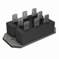
P102
Manufacturer Part Number
P102
Description
SCR HY-BRIDGE 600V 25A PACE-PAK
Manufacturer
Vishay
Specifications of P102
Structure
Bridge, Single Phase - SCRs/Diodes (Layout 1)
Number Of Scrs, Diodes
2 SCRs, 2 Diodes
Voltage - Off State
600V
Current - Gate Trigger (igt) (max)
60mA
Current - On State (it (rms)) (max)
25A (DC)
Current - Non Rep. Surge 50, 60hz (itsm)
357A, 375A
Current - Hold (ih) (max)
130mA
Mounting Type
Chassis Mount
Package / Case
6-PACE-PAK
Lead Free Status / RoHS Status
Lead free / RoHS Compliant
Current - On State (it (av)) (max)
-
Lead Free Status / Rohs Status
Details
Other names
*P102
Available stocks
Company
Part Number
Manufacturer
Quantity
Price

Company:
Part Number:
P1020NSE2DFB
Manufacturer:
Freescale Semiconductor
Quantity:
10 000
Company:
Part Number:
P1020NSE2FFB
Manufacturer:
Freescale Semiconductor
Quantity:
10 000
Company:
Part Number:
P1020NSE2HFB
Manufacturer:
FSL
Quantity:
27
Company:
Part Number:
P1020NSE2HFB
Manufacturer:
Freescale Semiconductor
Quantity:
10 000
Company:
Part Number:
P1020NSN2DFB
Manufacturer:
Freescale Semiconductor
Quantity:
10 000
Part Number:
P1020NSN2HFB
Manufacturer:
FREESCALE
Quantity:
20 000
Company:
Part Number:
P1020NXE2HFB
Manufacturer:
FSL
Quantity:
44
Part Number:
P1020NXE2HFB
Manufacturer:
FREESCALE
Quantity:
20 000
Company:
Part Number:
P1020NXN2HFB
Manufacturer:
FREESCA
Quantity:
1
Company:
Part Number:
P1020PSE2FDA
Manufacturer:
FSL
Quantity:
24


Triggering
Thermal and Mechanical Specification
Blocking
www.irf.com
T
T
R
R
T
wt
P
P
I
- V
V
I
V
I
dv/dt
I
I
I
V
GM
GD
GD
RRM
DRM
RRM
stg
J
GM
G(AV)
GT
GD
thJC
thCS
INS
GM
Parameter
Max. operating temperature range
Max. storage temperature range
Max. thermal resistance,
junction to case
Max. thermal resistance,
case to heatsink
Mounting torque, base to heatsink
Approximate weight
Parameter
Maximum peak gate power
Maximum average gate power
Maximum peak gate current
Maximum peak negative
gate voltage
Maximum gate voltage required
to trigger
Maximum gate current
required to trigger
Maximum gate voltage
that will not trigger
Maximum gate current
that will not trigger
Parameter
Maximum critical rate of rise of
off-state voltage
Max. peak reverse and off-state
leakage current at V
Max peak reverse leakage current
RMS isolation voltage
RRM
, V
DRM
-40 to 125
-40 to 125
58 (2.0)
P100
P100
P100
2500
2.24
0.10
200
100
90
60
35
0.2
10
10
8
2
2
3
2
1
4
2
Units Conditions
g (oz)
Units Conditions
Units Conditions
V/µs
K/W
K/W
mA
mA
µA
mA
Nm
°C
W
V
V
A
V
T
T
T
T
T
T
T
T
T
T
T
50Hz, circuit to base, all terminal shorted,
T
DC operation per junction
Mounting surface, smooth and greased
A mounting compound is recommended and the torque
should be checked after a period of 3 hours to allow for the
spread of the compound
J
J
J
J
J
J
J
J
J
J
J
J
= 125°C, rated V
= 125°C, rated V
= - 40°C
= 25°C
= 125°C
= - 40°C
= 25°C
= 125°C
= 125°C, exponential to 0.67 V
= 125°C, gate open circuit
= 25°C
= 25°C, t = 1s
Anode Supply = 6V resistive load
Anode Supply = 6V resistive load
DRM
DRM
Bulletin I27125 rev. A 04/99
applied
applied
P100 Series
DRM
gate open
3
Related parts for P102
Image
Part Number
Description
Manufacturer
Datasheet
Request
R

Part Number:
Description:
357-036-542-201 CARDEDGE 36POS DL .156 BLK LOPRO
Manufacturer:
Vishay
Datasheet:
Part Number:
Description:
357-036-542-201 CARDEDGE 36POS DL .156 BLK LOPRO
Manufacturer:
Vishay
Datasheet:
Part Number:
Description:
357-036-542-201 CARDEDGE 36POS DL .156 BLK LOPRO
Manufacturer:
Vishay
Datasheet:
Part Number:
Description:
357-036-542-201 CARDEDGE 36POS DL .156 BLK LOPRO
Manufacturer:
Vishay
Datasheet:
Part Number:
Description:
357-036-542-201 CARDEDGE 36POS DL .156 BLK LOPRO
Manufacturer:
Vishay
Datasheet:
Part Number:
Description:
357-036-542-201 CARDEDGE 36POS DL .156 BLK LOPRO
Manufacturer:
Vishay
Datasheet:
Part Number:
Description:
357-036-542-201 CARDEDGE 36POS DL .156 BLK LOPRO
Manufacturer:
Vishay
Datasheet:
Part Number:
Description:
357-036-542-201 CARDEDGE 36POS DL .156 BLK LOPRO
Manufacturer:
Vishay
Datasheet:
Part Number:
Description:
357-036-542-201 CARDEDGE 36POS DL .156 BLK LOPRO
Manufacturer:
Vishay
Datasheet:
Part Number:
Description:
357-036-542-201 CARDEDGE 36POS DL .156 BLK LOPRO
Manufacturer:
Vishay
Datasheet:
Part Number:
Description:
357-036-542-201 CARDEDGE 36POS DL .156 BLK LOPRO
Manufacturer:
Vishay
Datasheet:
Part Number:
Description:
357-036-542-201 CARDEDGE 36POS DL .156 BLK LOPRO
Manufacturer:
Vishay
Datasheet:
Part Number:
Description:
357-036-542-201 CARDEDGE 36POS DL .156 BLK LOPRO
Manufacturer:
Vishay
Datasheet:
Part Number:
Description:
357-036-542-201 CARDEDGE 36POS DL .156 BLK LOPRO
Manufacturer:
Vishay
Datasheet:
Part Number:
Description:
357-036-542-201 CARDEDGE 36POS DL .156 BLK LOPRO
Manufacturer:
Vishay
Datasheet: