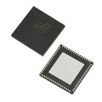
AS3991-BQFT austriamicrosystems, AS3991-BQFT Datasheet - Page 45

AS3991-BQFT
Manufacturer Part Number
AS3991-BQFT
Description
IC UHF RFID READER 64-QFN
Manufacturer
austriamicrosystems
Specifications of AS3991-BQFT
Rf Type
Read / Write
Frequency
840MHz ~ 960MHz
Features
ISO-18000-6
Package / Case
64-VFQFN, Exposed Pad
Lead Free Status / RoHS Status
Lead free / RoHS Compliant
Other names
AS3991-BQFT
AS3991-BQFTTR
AS3991-BQFTTR
AS3990/AS3991
Data Sheet - A p p l i c a t i o n I n f o r m a t i o n
Timing Requirements for Parallel Interface
While using parallel interface, there must always be a separation between CLK transitions and IO0…IO7 transitions.
Minimum time interval between transition on CLK and data lines is 100ns.
Minimum CLK high time interval is 300ns in periods when IO0…IO7 pins are used as data outputs
100ns in periods IO0…IO7 pins are used as inputs (address, command, or register write).
To decrease interferences between MCU communication and RF part of the chip, the output resistance of IO0…IO7
lines is 400Ω typical and 800Ω maximum. The firmware designer should be aware of the fact that in case higher
capacitance are connected to these pins, then possibly longer CLK high intervals are needed to allow settling of the
output level.
Serial Interface Communication
In serial interface IO4 pin enables the communication, CLK pin is serial data clock, IO7 is serial data input, and IO6 is
serial data output.
The interface is in reset as long the IO4 pin is high. Communication is started by falling edge on the IO4 pin. Data
coming from the host system is sampled on the falling of the CLK pin. When reading out the data from the UHF chip,
the data is set on the rising edge of the CLK pin. Host system (MCU) should sample the data on the falling edge on the
CLK pin. Communication is terminated by rising edge on the IO4 pin. All words are 8-bits long with the MSB
transmitted first.
Figure 9. Serial Interface Communication
In this mode the serial interface is in reset while the IO4 signal is high. CLK pin is serial data clock, IO7 is serial data in,
and IO6 is serial data output. Communication is terminated when IO4 signal goes high again.
Timing Requirements for Serial Interface
Minimum time interval between IO4 falling edge and first CLK change is 100ns.
Minimum CLK high time interval is 300ns in periods IO6 pin is used as data output (like register reading – data from
UHF chip to MCU) or 100ns in periods when IO7 pin is used as input (address, command, or register write – data from
MCU to UHF chip). Minimum CLK low interval is 100ns.
To decrease interferences between MCU communication and RF part of the chip the output resistance of IO6 line is
400Ω typical and 800Ω maximum. The firmware designer should be aware that in case of higher capacitance is
connected to this pin possibly longer CLK high interval is needed to allow settling of the output level.
Minimum time interval between last CLK falling edge and IO4 rising edge is 300ns.
www.austriamicrosystems.com
CLK
IO7
IO4
IO6
Start
condition
x
b7
b6
b5
b4
b3
b2
b1
b0
Revision 3.81
x
z7
z6
z5
z4
z3
z2
(see Figure 8)
z1
Stop
condition
z0
45 - 51
x
or


