TXM-900-HP3SPO Linx Technologies Inc, TXM-900-HP3SPO Datasheet - Page 3
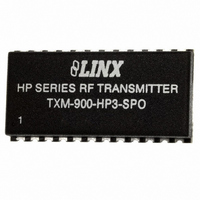
TXM-900-HP3SPO
Manufacturer Part Number
TXM-900-HP3SPO
Description
XMITTER RF 900MHZ 8-CH SMD
Manufacturer
Linx Technologies Inc
Datasheet
1.TXM-900-HP3SPO.pdf
(13 pages)
Specifications of TXM-900-HP3SPO
Frequency
902MHz ~ 928MHz
Modulation Or Protocol
FM, FSK
Data Rate - Maximum
56 kbps
Power - Output
3dBm
Current - Transmitting
14mA
Data Interface
PCB, Surface Mount
Antenna Connector
PCB, Surface Mount
Voltage - Supply
2.8 V ~ 13 V
Operating Temperature
-30°C ~ 85°C
Package / Case
10-SMD
Lead Free Status / RoHS Status
Lead free / RoHS Compliant
Features
-
Applications
-
Memory Size
-


Page 4
PIN ASSIGNMENTS
Figure 7: HP3 Series Receiver Pinout
14-19,
13, 20
21-24
SMD SIP
10
11
12
Pin #
1
2
3
4
5
6
7
8
9
10
1
2
3
4
5
6
7
8
9
Pinned Transmitter
CS1 / SS
CS2 / SS
Name
CLOCK
MODE
DATA
DATA
GND
GND
GND
ANT
CS0
CTS
PDN
V
NC
NC
CC
Clear-To-Send. This line will go high when the transmitter
Channel Select 1 / Serial Select Clock. Channel Select 1
Mode Select. GND for parallel channel selection, V
Channel Select 2 / Serial Select Data. Channel Select 2
Power Down. Pulling this line low will place the receiver
No Electrical Connection. Soldered for physical support
when in parallel channel selection mode, clock input for
No Electrical Connection. Soldered for physical support
when in parallel channel selection mode, data input for
into a low-current state. The module will not be able to
Digital / Analog Data Input. This line will output the
serial channel selection mode.
serial channel selection mode.
receive a signal in this state.
Analog Ground (SMD only)
Analog Ground (SMD only)
demodulated digital data.
is ready to accept data.
serial channel selection
50-ohm RF Output
Channel Select 0
only. (SMD only)
Description
Analog Ground
Supply Voltage
only.
Surface-Mount Transmitter
10
11
12
1
2
3
4
5
6
7
8
9
GND
ANT
GND
NC
CS0
CS1 / SS CLOCK
CS2 / SS DATA
CTS
PDN
VCC
MODE
DATA
GND
GND
NC
NC
NC
NC
NC
NC
NC
NC
NC
NC
CC
24
23
22
21
20
19
18
17
16
15
14
13
for
PIN DESCRIPTIONS
Figure 8: Pin Functions and Equivalent Circuits
14-19,
13, 20
21-24
SMD Pinned
1, 3
10
11
12
4,
2
5
6
7
8
9
Pin #
10
1
2
3
4
5
6
7
8
9
SS CLOCK
SS DATA
MODE
Name
DATA
CS1 /
CS2 /
GND
PDN
ANT
CS0
CTS
V
NC
CC
MODE
CS0
CS1
CS2
CTS
Out
Equivalent Circuit
PDN
Out
V
RF
100k
SMD (Only)
CC
430k
510k
50Ω
160k
20pF
25k
25k
25k
µ
µ
µ
25k
µ
No Electrical Connection
Voltage Input 2.8-13V
Digital / Analog Input
50-ohm RF Output
Serial Select Clock
Channel Select 1 /
Channel Select 2 /
Serial Select Data
Channel Select 0
Analog Ground
Clear-to-Send
Power Down
(Active Low)
Mode Select
Description
Output
Page 5
Related parts for TXM-900-HP3SPO
Image
Part Number
Description
Manufacturer
Datasheet
Request
R

Part Number:
Description:
TRANSMITTER RF 900MHZ 8-CHANNEL
Manufacturer:
Linx Technologies Inc
Datasheet:

Part Number:
Description:
TRANSMITTER RF 900MHZ 8-CHANNEL
Manufacturer:
Linx Technologies Inc
Datasheet:

Part Number:
Description:
TRANSMTR RF 900MHZ 8PAR/120SRLCH
Manufacturer:
Linx Technologies Inc
Datasheet:

Part Number:
Description:
TRANSMTR RF 902-928MHZ 8P/100S
Manufacturer:
Linx Technologies Inc
Datasheet:

Part Number:
Description:
RF Modules & Development Tools RF Transmitter 900MHz 8-CH SMD Pack
Manufacturer:
Linx Technologies Inc
Datasheet:

Part Number:
Description:
RF Modules & Development Tools RF Transmitter900MHz 8&100-CH SIP Pack
Manufacturer:
Linx Technologies Inc
Datasheet:
Part Number:
Description:
RF Modules & Development Tools RF Transmitter 900MHz 8-CH SIP Pack
Manufacturer:
Linx Technologies Inc
Datasheet:

Part Number:
Description:
HOLDER BATTERY 20MM COIN CR2032
Manufacturer:
Linx Technologies Inc
Datasheet:

Part Number:
Description:
CONN RPSMA BL CRJA-CPV 8.5" COAX
Manufacturer:
Linx Technologies Inc

Part Number:
Description:
CABLE RG174 RPSMA M/F 8.5"
Manufacturer:
Linx Technologies Inc

Part Number:
Description:
MODULE USB LOW SPEED
Manufacturer:
Linx Technologies Inc
Datasheet:

Part Number:
Description:
IC TRANSCODER MT BI-DIR 20-SSOP
Manufacturer:
Linx Technologies Inc
Datasheet:

Part Number:
Description:
IC ENCODER LOW SECURITY 8DIP
Manufacturer:
Linx Technologies Inc
Datasheet:

Part Number:
Description:
IC DECODER MS SERIES 20-SSOP
Manufacturer:
Linx Technologies Inc
Datasheet:
Part Number:
Description:
IC ENCODER MS SERIES 20-SSOP
Manufacturer:
Linx Technologies Inc
Datasheet: