TXM-916-ES_ Linx Technologies Inc, TXM-916-ES_ Datasheet - Page 4
TXM-916-ES_
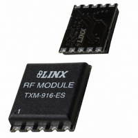
Manufacturer Part Number
TXM-916-ES_
Description
TRANSMITTER RF 916MHZ 10PIN SMD
Manufacturer
Linx Technologies Inc
Series
ESr
Datasheet
1.EVAL-916-ES.pdf
(11 pages)
Specifications of TXM-916-ES_
Frequency
916MHz
Applications
Home/Building Automation, Industrial Control and Monitoring
Modulation Or Protocol
AM, OOK
Data Rate - Maximum
56 kbps
Power - Output
4dBm
Current - Transmitting
8.5mA
Data Interface
PCB, Surface Mount
Antenna Connector
PCB, Surface Mount
Voltage - Supply
2.1 V ~ 4 V
Operating Temperature
0°C ~ 70°C
Package / Case
Module
Board Size
16 mm x 13 mm x 3.2 mm
Minimum Operating Temperature
0 C
Supply Voltage (min)
2.1 V
Product
RF Modules
Maximum Frequency
916.48 MHz
Supply Voltage (max)
4 V
Maximum Operating Temperature
+ 70 C
Lead Free Status / RoHS Status
Lead free / RoHS Compliant
Features
-
Memory Size
-
Lead Free Status / Rohs Status
Lead free / RoHS Compliant
Other names
TXM-916-ES
TXM-916-ES
TXM916ES
TXM-916-ES
TXM916ES


USING THE DIVIDED CLOCK OUTPUT (/CLK)
USING LADJ
Page 6
When the ES is used with a microcontroller, the divided clock output (/CLK)
saves cost and space by eliminating the need for a crystal or other frequency
reference for the microprocessor. This line is an open collector output, so an
external pull-up resistor (R
positive supply voltage. The value of R
1) Determine the clock frequency (f
will be the Tx center frequency (in MHz) divided by 1,024; if /CLK SEL is
grounded, it will be /256.
2) Determine the load capacitance of the PCB plus the microcontroller’s input
capacitance (C
Using these two factors, the value of R
“/256” R
Example:
For /256: 1000/((916.48/256)x8x5)=6.98kΩ For /1024: 1000/((916.48/1024)x8x5)=27.9kΩ
The transmitter’s output power can be externally adjusted by approximately
-65dBm using the LADJ line. This eliminates the need for external attenuation
and allows the transmitter’s power to be easily adjusted for range control, lower
power consumption, or to meet legal requirements. This line can also be
modulated to allow the ES to operate as an AM transmitter; however, this is not
recommended since the ES receiver is designed only for FM / FSK recovery and
the performance and noise immunity advantages of FM would be lost.
When the LADJ line is open, the output power will be at its maximum and the
transmitter will draw 7mA typically. When LADJ is at 0V, the output power will be
at its minimum and the transmitter will draw 3mA typically.
To set the transmit power at a particular level, simply create a voltage reference
at the LADJ line at an appropriate level to achieve the desired output power. The
easiest way to accomplish this is with an appropriate value resistor from the
LADJ line to ground. This resistor works in combination with the internal supply
pull-up to create a voltage divider. Page 3 of this data guide features a chart
showing typical resistor values and corresponding attenuation levels.
The LADJ line is very useful during FCC testing to compensate for antenna gain
or other product-specific issues that may cause the output power to exceed legal
limits. Often it is wise to connect the LADJ line to a variable resistor so that the
test lab can precisely adjust the output power to the maximum threshold allowed
by law. The resistor’s value can then be noted and a fixed resistor substituted for
final testing. Even in designs where attenuation is not anticipated, it is a good
idea to place a resistor pad connected to LADJ so that it can be used if needed.
For more sophisticated designs, LADJ may also be controlled by a DAC or digital
potentiometer to allow precise and digitally variable output power control.
In any case where the voltage on the LADJ line may fall below 1.5VDC, a low-
value ceramic capacitor (200 to 4,700pF) must be placed from the module’s
power supply to the LADJ pin. This is necessary to meet the module’s minimum
enable voltage at start-up.
L
= 1000/(f
LD
in pF).
CLKOUT
*8*C
L
) should be connected between this line and the
LD
)
CLKOUT
L
L
“/1024” R
Example:
is calculated using two factors:
can be easily calculated:
). If /CLK SE is open, the /CLK output
L
= 1000/(f
CLKOUT
*8*C
LD
)
USING THE PDN PIN
USING THE LO_V_D PIN
POWER SUPPLY REQUIREMENTS
The Power Down (PDN) line can be used to power down the transmitter without
the need for an external switch. This line has an internal pull-up, so when it is
held high or simply left floating, the module will be active.
When the PDN line is pulled to ground, the transmitter will enter into a low-
current (<95µA) power-down mode. During this time, the transmitter is off and
cannot perform any function. The startup time coming out of power-down will be
the same as applying V
The PDN line allows easy control of the transmitter state from external
components, such as a microcontroller. By periodically activating the transmitter,
sending data, then powering down, the transmitter’s average current
consumption can be greatly reduced, saving power in battery operated
applications.
In many instances, the transmitter may be employed in a battery-powered
device. In such applications, it is often useful to be able to sense a low-battery
condition, either to signal the need for battery replacement or to power down
components that might otherwise operate unpredictably. Normally, this
supervisory function would require additional circuitry, but the ES Series
transmitter includes the function on-board.
The Low Voltage Detect line (LO_V_D) will transition low when the supply
voltage to the transmitter falls below a typical threshold of 2.15VDC. This output
can be tied directly to the module’s PDN line to shut off the transmitter, or used
to indicate the low voltage condition to an external circuit or microprocessor. The
output could also be used to provide a visual indication of the low power
condition via a LED, although a buffer transistor would generally be required to
provide an adequate drive level.
The output can also be monitored in applications with a power supply as a
safeguard against brownout conditions.
The module does not have an internal voltage
regulator; therefore it requires a clean, well-regulated
power source. While it is preferable to power the unit
from a battery, it can also be operated from a power
supply as long as noise is less than 20mV. Power
supply noise can affect the transmitter modulation;
therefore, providing a clean power supply for the
module should be a high priority during design.
A 10Ω resistor in series with the supply followed by a
10µF tantalum capacitor from V
of supply power is poor. Note that operation from 4.3 to 5.2 volts requires the
use of an external 270Ω resistor placed in series with the supply to prevent V
from exceeding 4.0 volts, so the dropping resistor can take the place of the 10Ω
resistor in the supply filter. These values may need to be adjusted depending on
the noise present on the supply line.
CC
.
CC
to ground will help in cases where the quality
Figure 9: Supply Filter
Vcc IN
10Ω
Vcc TO
MODULE
+
Page 7
10μF
CC
Related parts for TXM-916-ES_
Image
Part Number
Description
Manufacturer
Datasheet
Request
R

Part Number:
Description:
TRANSMITTER RF 418MHZ SMT
Manufacturer:
Linx Technologies Inc
Datasheet:

Part Number:
Description:
XMITTER RF 869MHZ 10PIN SMD
Manufacturer:
Linx Technologies Inc
Datasheet:

Part Number:
Description:
TRANSMITTER RF 900MHZ 8-CHANNEL
Manufacturer:
Linx Technologies Inc
Datasheet:

Part Number:
Description:
TRANSMITTER RF 433MHZ SMT
Manufacturer:
Linx Technologies Inc
Datasheet:

Part Number:
Description:
TRANSMITTER 433MHZ LR SERIES
Manufacturer:
Linx Technologies Inc
Datasheet:

Part Number:
Description:
TRANSMITTER 418MHZ LR SERIES
Manufacturer:
Linx Technologies Inc
Datasheet:

Part Number:
Description:
TRANSMITTER RF 900MHZ 8-CHANNEL
Manufacturer:
Linx Technologies Inc
Datasheet:

Part Number:
Description:
TRANSMTR RF 900MHZ 8PAR/120SRLCH
Manufacturer:
Linx Technologies Inc
Datasheet:

Part Number:
Description:
TRANSMITTER 315MHZ LR SERIES
Manufacturer:
Linx Technologies Inc
Datasheet:

Part Number:
Description:
TRANSMITTER RF 315MHZ SMT
Manufacturer:
Linx Technologies Inc
Datasheet:

Part Number:
Description:
MODULE USB LOW SPEED
Manufacturer:
Linx Technologies Inc
Datasheet:

Part Number:
Description:
IC TRANSCODER MT BI-DIR 20-SSOP
Manufacturer:
Linx Technologies Inc
Datasheet:

Part Number:
Description:
IC ENCODER LOW SECURITY 8DIP
Manufacturer:
Linx Technologies Inc
Datasheet:

Part Number:
Description:
IC DECODER MS SERIES 20-SSOP
Manufacturer:
Linx Technologies Inc
Datasheet:
Part Number:
Description:
IC ENCODER MS SERIES 20-SSOP
Manufacturer:
Linx Technologies Inc
Datasheet: