TXM-418-LC_ Linx Technologies Inc, TXM-418-LC_ Datasheet - Page 4
TXM-418-LC_
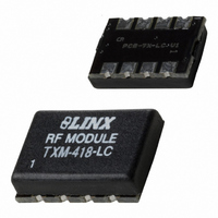
Manufacturer Part Number
TXM-418-LC_
Description
TRANSMITTER RF 418MHZ SMT
Manufacturer
Linx Technologies Inc
Series
LCr
Specifications of TXM-418-LC_
Frequency
418MHz
Applications
ISM, RKE, Security and Fire Alarms
Modulation Or Protocol
ASK, FSK
Data Rate - Maximum
5 kbps
Power - Output
-4dBm ~ 4dBm
Current - Transmitting
3mA
Data Interface
PCB, Surface Mount
Antenna Connector
PCB, Surface Mount
Voltage - Supply
2.7 V ~ 5.2 V
Operating Temperature
-30°C ~ 70°C
Package / Case
Surface Mount
Board Size
12.7 mm x 9.1 mm x 3.3 mm
Minimum Operating Temperature
- 40 C
Supply Voltage (min)
2.1 V
Product
RF Modules
Maximum Frequency
418 MHz
Supply Voltage (max)
3.6 V
Maximum Operating Temperature
+ 85 C
Lead Free Status / RoHS Status
Lead free / RoHS Compliant
Features
-
Memory Size
-
Lead Free Status / Rohs Status
Lead free / RoHS Compliant
Other names
TXM-418-LC
TXM-418-LC
TXM-418-LC-R
TXM-418-LC
TXM-418-LC-R


THE DATA INPUT
ADJUSTING THE OUTPUT POWER
Figure 10: A T-Pad Attenuator Layout Example
Page 6
A CMOS / TTL level data input is provided on Pin 2. This line is normally supplied
with a serial bitstream input directly from a microprocessor, encoder, or UART.
During standby, or the input of a logic low, the carrier is fully suppressed and the
transmitter consumes less than 2µA of current. During a logic high, the
transmitter generates a carrier to indicate to the receiver the presence of a logic
‘1’. The applied data should not exceed a rate of 5,000bps. The data input line
should always be driven with a voltage common to the supply voltage present on
Pin 7 (V
Depending on the type of antenna being used and the duty cycle of the data, the
output power of the LC Series transmitter module may be higher than FCC
regulations allow. The output power of the module is intentionally set high to
compensate for losses resulting from inefficient antennas that may be used to
realize cost or space savings. Since attenuation is often required, it is generally
wise to provide for its implementation and allow the FCC test lab to easily
attenuate the transmitter to the maximum legal limit for your product.
Two methods of atten uation are available using the LC Series transmitter
module. First, a resistor may be placed between Pin 4 (LADJ) and ground to
achieve up to a 7dB reduction in output power. The resistor value is easily
determined from Figure 7 on Page 3. Do not exceed the resistance values shown
as trans mitter instability may result. This method can also be used to reduce the
transmission range and power consumption.
Another method com monly used to achieve attenuation, particularly at higher
levels, is the use of a T-pad attenuator. A T-pad is a network of three resistors
that allows for variable attenuation while main taining the correct match to the
antenna. It is usually prudent to allow space for the addition of a T-pad. An
example of a T-pad attenuator layout is shown in the figure below. For further
details on T-pad attenuators, please refer to Application Note AN-00150.
ANT
CC
CIRCUIT
ANT OUT
R1
R1
) and should never be allowed to exceed the supply voltage.
R2
GND
PADS FOR SMD
PADS FOR SMD
PADS FOR SMD
RESISTORS
RESISTORS
RESISTORS
WITH PROVISION FOR ATTENUATION
TYPICAL LAYOUT
ANT
GROUND PLANE
GROUND PLANE
GROUND PLANE
ON LOWER LAYER
ON LOWER LAYER
ON LOWER LAYER
GROUND
GROUND
GROUND
GROUND
GROUND
GROUND
POWER SUPPLY REQUIREMENTS
TRANSMITTING DATA
The module does not have an internal voltage regulator; therefore it requires a
clean, well-regulated power source. While it is preferable to power the unit from
a battery, the unit can also be operated from a power supply as long as noise is
less than 20mV. Power supply noise can significantly
affect the transmitter modulation; therefore, providing
a clean power supply for the module should be a high
design priority.
A 10Ω resistor in series with the supply followed by a
10µF tantalum capacitor from V
in cases where the quality of supply power is poor.
These values may need to be adjusted depending on
the noise present on the supply line.
Once a reliable RF link has been established, the challenge becomes how to
effectively transfer data across it. While a properly designed RF link provides
reliable data transfer under most conditions, there are still distinct differences
from a wired link that must be addressed. Since the LC Series modules do not
incorporate internal encoding or decoding, a user has tremendous flexibility in
how data is handled.
If you want to transfer simple control or status signals, such as button presses or
switch closures, and your product does not have a microprocessor on board, or
you wish to avoid protocol development, consider using an encoder and decoder
IC set. These chips are available from a range of manufacturers, including Linx.
They take care of all encoding and decoding functions and generally provide a
number of data pins to which switches can be directly connected. In addition,
address bits are usually provided for security and to allow the addressing of
multiple units independently. These ICs are an excellent way to bring basic
remote control / status products to market quickly and inexpensively.
Additionally, it is a simple task to interface with inexpensive microprocessors,
such as the Microchip PIC, or one of many IR, remote control, or modem ICs.
It is always important to separate what types of transmissions are technically
possible from those that are legally allowable in the country of intended
operation. While the LR Series is ideally suited to the long range transfer of
control and command information, it can also be used with great success for the
transfer of true variable data such as temperature, pressure, or sensor data.
However, the 260 - 470MHz band in which the module operates is regulated by
Part 15, Section 231 of the FCC regulations. Many types of transmissions,
especially those involving automatic transmissions or variable data, may need to
be periodic. You may wish to review Application Notes AN-00125 and AN-00140
along with Part 15, Section 231 of the FCC regulations for further details on
acceptable transmission content in the Unites States.
Another area of consideration is that of data structure or protocol. The data
should be formatted in a predictable way and should be able to deal with errors
due to interference. This will ensure that the data is received and interpreted
correctly. If you are not familiar with the considerations for sending serial data in
a wireless environment, you will want to review Application Note AN-00160.
CC
to ground will help
Figure 11: Supply Filter
Vcc IN
10Ω
Vcc TO
MODULE
+
Page 7
10μF
Related parts for TXM-418-LC_
Image
Part Number
Description
Manufacturer
Datasheet
Request
R

Part Number:
Description:
TRANSMITTER 418MHZ LR SERIES
Manufacturer:
Linx Technologies Inc
Datasheet:

Part Number:
Description:
TRANSMITTER RF 418MHZ
Manufacturer:
Linx Technologies Inc
Datasheet:

Part Number:
Description:
TRANSMITTER RF 916MHZ 10PIN SMD
Manufacturer:
Linx Technologies Inc
Datasheet:

Part Number:
Description:
XMITTER RF 869MHZ 10PIN SMD
Manufacturer:
Linx Technologies Inc
Datasheet:
Part Number:
Description:
TRANSMITTER RF 900MHZ 8-CHANNEL
Manufacturer:
Linx Technologies Inc
Datasheet:

Part Number:
Description:
TRANSMITTER RF 433MHZ SMT
Manufacturer:
Linx Technologies Inc
Datasheet:

Part Number:
Description:
TRANSMITTER 433MHZ LR SERIES
Manufacturer:
Linx Technologies Inc
Datasheet:

Part Number:
Description:
TRANSMITTER RF 900MHZ 8-CHANNEL
Manufacturer:
Linx Technologies Inc
Datasheet:

Part Number:
Description:
TRANSMTR RF 900MHZ 8PAR/120SRLCH
Manufacturer:
Linx Technologies Inc
Datasheet:

Part Number:
Description:
TRANSMITTER 315MHZ LR SERIES
Manufacturer:
Linx Technologies Inc
Datasheet:

Part Number:
Description:
MODULE USB LOW SPEED
Manufacturer:
Linx Technologies Inc
Datasheet:

Part Number:
Description:
IC TRANSCODER MT BI-DIR 20-SSOP
Manufacturer:
Linx Technologies Inc
Datasheet:

Part Number:
Description:
IC ENCODER LOW SECURITY 8DIP
Manufacturer:
Linx Technologies Inc
Datasheet:

Part Number:
Description:
IC DECODER MS SERIES 20-SSOP
Manufacturer:
Linx Technologies Inc
Datasheet:
Part Number:
Description:
IC ENCODER MS SERIES 20-SSOP
Manufacturer:
Linx Technologies Inc
Datasheet: