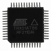
AT86RF211DAI Atmel, AT86RF211DAI Datasheet - Page 9

AT86RF211DAI
Manufacturer Part Number
AT86RF211DAI
Description
IC RF TXRX FSK 400-950MHZ 48TQFP
Manufacturer
Atmel
Datasheet
1.AT86RF211DB-433LT.pdf
(19 pages)
Specifications of AT86RF211DAI
Frequency
400MHz ~ 950MHz
Data Rate - Maximum
100kbps
Modulation Or Protocol
FSK
Applications
ISM
Power - Output
7dBm ~ 12dBm
Sensitivity
-107dBm
Voltage - Supply
2.4 V ~ 3.6 V
Data Interface
PCB, Surface Mount
Antenna Connector
PCB, Surface Mount
Operating Temperature
-40°C ~ 85°C
Package / Case
48-TQFP Exposed Pad, 48-eTQFP, 48-HTQFP, 48-VQFP
Lead Free Status / RoHS Status
Contains lead / RoHS non-compliant
Memory Size
-
Current - Transmitting
-
Current - Receiving
-
Clock Recovery of the Wake-up
Error Detection
2186A–WIRE–08/02
This clock recovery process must not be confused with the clock recovery of the normal
communication receive mode, giving an output clock on DATACLK pin. The wake-up
clock recovery gives no output signal. It has only the purpose to trigger the received
Address and Data fields. The data rate of the received Header is automatically extracted
from a correct Header:
•
•
The RATECHK functionality MUST BE USED with the wake-up procedure. It is manda-
tory to ensure no detection of compatible random sequence in noise when no signal is
present. The RSSI level allows to remove the effect and the RATECHK helps to get the
best concerning sensitivity.
Error detection is implemented when MSGTST (of WUC register) is set to '1'. This is
useful when debugging wake-up protocol.
After correct header readout, the reception of message is interrupted if the received
Address does not fit or if an error is detected (in order to be analyzed):
•
•
•
•
Note:
if RATECHK (WUR register) is set to '1', the extracted data rate is compared to
RATE (of WUR register) with a tolerance of ± RATETOL (WUR register). If the
checking process succeeds, the message is considered valid. The advised
tolerance for the data rate must be lower than 25% of the data rate (typically 10%).
if RATECHK is set to '1' and the extracted data rate is different from the
programmed one with the relevant tolerance, the detected Header is ignored and
the chip searches for another message until the end of WL2 period. This option
allows the designer to wake-up different devices with only the Header: no Address
and no Data, but different data rates. It also helps to remove Header sequence
which may occur randomly during scan period.
wrong Address value.
wrong rate in RATECHK mode.
no STOP field in variable data length mode.
stuff error if four consecutive equal bits in the field (Address + Data) are detected.
there is no direct access to the received Address in the chip. To help debug, set ADDL
(of WUA) to 0 and DATL (of WUC) to Address length: the Address is then caught as a
Data!
AT86RF211 (TRX01)
9


