TR3005 RFM, TR3005 Datasheet - Page 8
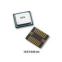
TR3005
Manufacturer Part Number
TR3005
Description
ASH TR 115.2 KBPS 403.5 MHZ
Manufacturer
RFM
Series
TRr
Datasheet
1.TR3005.pdf
(12 pages)
Specifications of TR3005
Frequency
403.55MHz
Data Rate - Maximum
115.2kbps
Modulation Or Protocol
ASK, OOK
Applications
ISM
Power - Output
0dBm
Sensitivity
-109dBm
Voltage - Supply
2.2 V ~ 3.7 V
Current - Receiving
3.8mA
Current - Transmitting
7.5mA
Data Interface
PCB, Surface Mount
Antenna Connector
PCB, Surface Mount
Operating Temperature
-10°C ~ 55°C
Package / Case
SM-20H
Wireless Frequency
403.5 MHz
Operating Supply Voltage
2.5 V, 3.3 V
Maximum Operating Temperature
+ 85 C
Mounting Style
SMD/SMT
Maximum Data Rate
115.2 Kbps
Minimum Operating Temperature
- 10 C
Modulation
OOK/ASK
Lead Free Status / RoHS Status
Lead free by exemption / RoHS compliant by exemption
Memory Size
-
Lead Free Status / Rohs Status
Lead free / RoHS Compliant
Other names
583-1090-2


Trans ceiver Event Tim ing, 3.0 Vdc, -40 to +85
Turn On to Re ceive
Turn On to TXOOK
Turn On to TXASK
RX to TXOOK
RX to TXASK
TXOOK to RX
TXASK to RX
Sleep to RX
Sleep to TXOOK
Sleep to TXASK
RX to Sleep
TXOOK to Sleep
TXASK to Sleep
AGC En gage
AGC Hold-In
PKDET At tack Time Con stant
PKDET De cay Time Con stant
PRATE In ter val
PWIDTH RFA1
PWIDTH RFA2
PRATE Cy cle
PWIDTH High (RFA1 & RFA2)
LPF Group De lay
LPF 3 dB Band width
BBOUT-CMPIN Time Con stant
Event
Symbol
t
t
t
t
t
t
t
t
t
t
t
t
t
t
t
t
t
t
t
f
t
t
t
t
t
AGC
AGH
PW1
PW2
PWH
PTO
PTA
RTO
RTA
TOR
TAR
STO
STA
TOS
TAS
PKA
PKD
PRC
FGD
BBC
PRI
LPF
PR
SR
RS
0
C
0.05 to 0.55 µs
3*t
0.1 to 1.1 µs
0.55 to 1 µs
0.064*C
0.1 to 5 µs
C
1445/R
C
1000*t
1750/f
BBC
1.1*t
PKD
15 ms
15 ms
AGC/
12 µs
12 µs
3*t
3*t
3*t
16 µs
16 µs
10 µs
10 µs
10 µs
Time
5 µs
+ 15 ms
/4167
BBC
BBC
BBC
19.1
PW1
PKA
LPF
LPF
BBO
Min/Max
range
range
range
range
range
max
max
max
max
max
max
max
max
max
max
max
max
max
max
max
min
min
min
min
min
Ta ble 1
1µs CNTRL0/CNTROL1 rise times
1µs CNTRL0/CNTROL1 fall times
10 ms supply voltage rise time
10 ms supply voltage rise time
10 ms supply voltage rise time
1 µs rise time, -30 dBm signal
f
LPF
1 µs CNTRL1 rise time
1 µs CNTRL0 rise time
1 µs CNTRL0 rise time
1 µs CNTRL1 rise time
CAGC in pF, t
1 µs CNTRL1 fall time
1 µs CNTRL0 fall time
1 µs CNTRL0 fall time
1 µs CNTRL1 fall time
C
t
t
low data rate mode
low data rate mode
low data rate mode
high data rate mode
high data rate mode
FGD
BBC
in kHz, R
PKD
t
Test Conditions
PKD
in µs, f
in µs, C
in pF, t
and t
LPF
PKA
LPF
BBO
PKA
AGH
in kilohms
in µs
in kHz
in pF
in µs
in µs
time until transceiver is in power-down mode
time until transceiver is in power-down mode
time until transceiver is in power-down mode
time until TXMOD can modulate transmitter
time until TXMOD can modulate transmitter
time until TXMOD can modulate transmitter
time until TXMOD can modulate transmitter
TXMOD low 1 µs before CNTRL1 falls
TXMOD low 1 µs before CNTRL0 falls
RFA1 switches from 35 to 5 dB gain
time until receiver operational
time until receiver operational
time until receiver operational
time until receiver operational
user selected; longer than t
slaved to attack time
user selected mode
user selected mode
user selected mode
user selected mode
user selected mode
user selected
user selected
user selected
user selected
Notes
PKD
Related parts for TR3005
Image
Part Number
Description
Manufacturer
Datasheet
Request
R

Part Number:
Description:
TRANSCEIVER RF 916MHZ 1/2-DUPLEX
Manufacturer:
Linx Technologies Inc
Datasheet:
Part Number:
Description:
TRANSCEIVER RF 916MHZ 1/2-DUPLEX
Manufacturer:
Linx Technologies Inc
Datasheet:
Part Number:
Description:
TXCVR RF 900MHZ 1/2-DUPLEX 180CH
Manufacturer:
Linx Technologies Inc
Part Number:
Description:
TRANSCEIVER RF 916MHZ 20PIN SMD
Manufacturer:
Linx Technologies Inc
Datasheet:

Part Number:
Description:
ASH TR 115.2 KBPS 433.92 MHZ
Manufacturer:
RFM
Datasheet:

Part Number:
Description:
ASH TR 115.2 KBPS 916.5 MHZ
Manufacturer:
RFM
Datasheet:

Part Number:
Description:
ASH TR 115.2 KBPS 433.92 MHZ
Manufacturer:
RFM
Datasheet:
Part Number:
Description:
ASH TR 115.2 KBPS 916.5 MHZ
Manufacturer:
RFM
Datasheet:

Part Number:
Description:
ASH RX 115.2 KBPS 433.92 MHZ
Manufacturer:
RFM
Datasheet:

Part Number:
Description:
RFIC TRANCEIVER MULTI-CHANNEL FS
Manufacturer:
RFM
Datasheet:
Part Number:
Description:
10-Terminal Ceramic Surface-Mount Case 7 x 5 mm Nominal Footprint
Manufacturer:
RFM [RF Monolithics, Inc]
Datasheet:
Part Number:
Description:
QUAD-BAND GSM850/GSM/DCS/PCS POWER AMP MODULE
Manufacturer:
RFM [RF Monolithics, Inc]
Datasheet:
Part Number:
Description:
402 to 405 MHz Medical Band Front-end Filter
Manufacturer:
RFM [RF Monolithics, Inc]
Datasheet:
Part Number:
Description:
674.03 MHz SAW Resonator
Manufacturer:
RFM [RF Monolithics, Inc]
Datasheet: