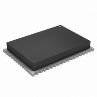
ATZB-24-B0 Atmel, ATZB-24-B0 Datasheet - Page 14

ATZB-24-B0
Manufacturer Part Number
ATZB-24-B0
Description
KIT MOD 802.15.4/ZIGB 2.4GHZ RF
Manufacturer
Atmel
Datasheet
1.ATZB-24-B0R.pdf
(28 pages)
Specifications of ATZB-24-B0
Frequency
2.4GHz
Data Rate - Maximum
250kbps
Modulation Or Protocol
802.15.4 Zigbee
Applications
Home/Building Automation, Industrial Control and Monitoring
Power - Output
3dBm
Sensitivity
-101dBm
Voltage - Supply
1.8 V ~ 3.6 V
Current - Receiving
19mA
Current - Transmitting
18mA
Data Interface
PCB, Surface Mount
Memory Size
128kBytes Flash, 8kBytes RAM, 4kBytes EEPROM
Antenna Connector
PCB, Surface Mount
Operating Temperature
-40°C ~ 85°C
Package / Case
Module
Lead Free Status / RoHS Status
Lead free / RoHS Compliant
Available stocks
Company
Part Number
Manufacturer
Quantity
Price
Company:
Part Number:
ATZB-24-B0R
Manufacturer:
NUVOTON
Quantity:
1 001
ZigBit™ 2.4 GHz Wireless Modules
Table 3-6. Pin descriptions
Connector
9,22,23
24,25
Pin
10
11
12
13
14
15
16
17
18
19
20
21
26
27
28
29
30
31
32
33
34
1
2
3
4
5
6
7
8
ADC_INPUT_3
ADC_INPUT_2
ADC_INPUT_1
OSC32K_OUT
UART_RXD
UART_TXD
UART_RTS
UART_CTS
JTAG_TMS
JTAG_TDO
JTAG_TCK
SPI_MISO
SPI_MOSI
Pin Name
CPU_CLK
I2C_DATA
JTAG_TDI
SPI_CLK
I2C_CLK
A_VREF
RESET
D_VCC
GPIO0
GPIO1
GPIO2
GPIO6
GPIO7
GPIO3
GPIO4
GPIO5
DGND
BAT
RF clock output. When module is in active state, 4
MHz signal is present on this line. While module is
RTS input (Request to send) for UART hardware
General Purpose digital Input/Output 0
General Purpose digital Input/Output 1
General Purpose digital Input/Output 2
General Purpose digital Input/Output 6
General Purpose digital Input/Output 7
General Purpose digital Input/Output 3
General Purpose digital Input/Output 4
General Purpose digital Input/Output 5
CTS output (Clear to send) for UART hardware
in the sleeping state, clock generation is also
measurement. This pin equals V
ADC Input Channel 0, used for battery level
Input/Output reference voltage for ADC
I
2
flow control. Active low
C Serial data input/output
UART transmit output
JTAG Test Mode Select
JTAG Test Data Output
flow control. Active low
Reserved for stack operation
Reserved for stack operation
Reserved for stack operation
I
UART receive input
Digital Supply Voltage (V
2
JTAG Test Data Input
32.768 kHz clock output
C Serial clock output
ADC Input Channel 3
ADC Input Channel 2
ADC Input Channel 1
Reset input (active low)
JTAG Test Clock
Digital Ground
Description
stopped
(4)
(2)(3)(4)(6)
(1)(2)(3)(4)(7)
.
(1)(2)(3)(4)(7)
(2)(3)(4)(7)(8)
(2)(3)(4)(6)
(2)(3)(4)(7)
(2)(3)(4)(7)
(2)(3)(4)(6)
(2)(3)(4)(6)
(2)(3)(7)
(2)(3)(7)
(2)(3)(7)
(2)(3)(4)(7)
(4)(5)
CC
(4)
CC
)
(9)
/3.
(4)
(4)
(4)
(2)(3)(4)(7)
(2)(3)(4)(7)
(2)(3)(4)(7)
(2)(3)(4)(7)
(2)(3)(4)(7)
(2)(3)(4)(7)
(2)(3)(4)(7)
(2)(3)(4)(7)
(2)(3)(7)
8226B–MCU Wireless–06/09
I/O
I/O
I/O
I/O
I/O
I/O
I/O
I/O
I/O
I/O
I/O
I/O
I/O
O
O
O
O
O
O
O
I
I
I
I
I
I
I
I
I
Specifications
State after
Power on
Default
tri-state
tri-state
tri-state
tri-state
tri-state
tri-state
tri-state
tri-state
tri-state
tri-state
tri-state
tri-state
tri-state
tri-state
tri-state
tri-state
tri-state
tri-state
tri-state
3-11


