XM1205C433XE1 Semtech, XM1205C433XE1 Datasheet - Page 2
XM1205C433XE1
Manufacturer Part Number
XM1205C433XE1
Description
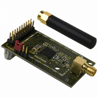
MODULE TXRX TRUE RF 433MHZ
Manufacturer
Semtech
Datasheet
1.XM1205C433XE1.pdf
(2 pages)
Specifications of XM1205C433XE1
Frequency
433MHz
Data Rate - Maximum
152.3kbps
Modulation Or Protocol
FSK
Applications
AMR, ISM, Home Automation, Process Control
Power - Output
0 ~ 15dBm
Sensitivity
-121dBm
Voltage - Supply
2.4 V ~ 3.6 V
Current - Receiving
14mA
Current - Transmitting
62mA
Data Interface
Connector, 2 x 10 Header
Antenna Connector
RP-SMA
Package / Case
Module
Lead Free Status / RoHS Status
Contains lead / RoHS non-compliant
Operating Temperature
-
Memory Size
-


©XEMICS 2004
All rights reserved. Reproduction in whole or in part is prohibited without the prior written consent of the copyright owner. The information
presented in this document does not form part of any quotation or contract, is believed to be accurate and reliable and may be changed without
notice. No liability will be accepted by the publisher for any consequence of its use. Publication thereof does not convey nor imply any license
under patent or other industrial or intellectual property rights. TrueRF™ is a XEMICS trademark.
I/O LINES
The XM1205 can be connected to the main
application board, test equipment or XEMICS
development tools via a 20 pins connector shown in
the figure below.
Pin #1
"SCK": (Input), Serial Clock line, used to set-up
configuration of the XE1205 transceiver IC.
Pin #2
"VDD": Connect to a 3.3V power supply.
Pin #3
"MOSI": (Input), SPI Master Output Slave Input.
Pin #4
"GND": Connect to Ground
Pin #5
"IRQ1": (Output), Interrupt: DCLK / FIFOFULL.
Pin #6
NC.
Pin #7
"NSS_CONFIG": (Input), SPI Select Configuration.
Pin #8
"MISO": (Output), SPI Master Input Slave Output.
Pin #9
"CLKOUT": (Output), Output clock at reference
frequency divided by 4, 8, 16, 32.
Pin #10
NC.
2
Pin #11
“SW(0)”, (Input / Output) Transmit/Receive/Stand-
by/Sleep Mode Select
Pin #12
"IRQ_0": (Output), Interrupt: PATTERN / FIFOEMPTY
Pin #13
“SW(1)”, (Input / Output) Transmit/Receive/Stand-
by/Sleep Mode Select
Pin #14
NC
Pin #15
"IRQ1": (Output), Interrupt: DCLK / FIFOFULL
Pin #16
NC
Pin #17
"DATA": (Input / Output), Transmitter input data or
Receiver output data.
Pin #18
NC
Pin #19
"NS_DATA": (Input), SPI Select DATA / DATAIN.
Pin #20
NC
For convenience, the XM1205 can be supplied through
separate VDD and GND pins. In this case, the two
supply lines of the 20-pin connector should not be
used, the jumper "VDD1" should be removed.
GND NC
VDD
« VDD1 »
Jumper
11
13
15
17
19
1
3
5
7
9
VDD_ext
10
12
14
16
18
20
2
4
6
8
Product Brief
XM1205 TrueRF™ Module
PB0410-279
Related parts for XM1205C433XE1
Image
Part Number
Description
Manufacturer
Datasheet
Request
R

Part Number:
Description:
EVALUATION BOARD
Manufacturer:
Semtech
Datasheet:
Part Number:
Description:
EVALUATION BOARD
Manufacturer:
Semtech
Datasheet:
Part Number:
Description:
VOLTAGE SUPPRESSOR, TRANSIENT SEMTECH
Manufacturer:
Semtech
Datasheet:

Part Number:
Description:
HIGH VOLTAGE CAPACITORS MONOLITHIC CERAMIC TYPE
Manufacturer:
Semtech Corporation
Datasheet:
Part Number:
Description:
EZ1084CM5.0 AMP POSITIVE VOLTAGE REGULATOR
Manufacturer:
Semtech Corporation
Datasheet:
Part Number:
Description:
3.0 AMP LOW DROPOUT POSITIVE VOLTAGE REGULATORS
Manufacturer:
Semtech Corporation
Datasheet:
Part Number:
Description:
Manufacturer:
Semtech Corporation
Datasheet:
Part Number:
Description:
RailClamp Low Capacitance TVS Diode Array
Manufacturer:
Semtech Corporation
Datasheet:
Part Number:
Description:
Manufacturer:
Semtech Corporation
Datasheet:
Part Number:
Description:
Manufacturer:
Semtech Corporation
Datasheet:
Part Number:
Description:
Manufacturer:
Semtech Corporation
Datasheet:
Part Number:
Description:
Manufacturer:
Semtech Corporation
Datasheet: