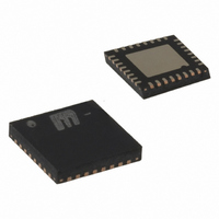
MICRF507YML TR Micrel Inc, MICRF507YML TR Datasheet - Page 30

MICRF507YML TR
Manufacturer Part Number
MICRF507YML TR
Description
TXRX FSK LOW PWR W/AMP 32MLF
Manufacturer
Micrel Inc
Series
RadioWire®r
Datasheet
1.MICRF507YML_TR.pdf
(46 pages)
Specifications of MICRF507YML TR
Frequency
470MHz ~ 510MHz
Data Rate - Maximum
200kbps
Modulation Or Protocol
FSK
Applications
AMR, ISM, SRD
Power - Output
10dBm
Sensitivity
-113dBm
Voltage - Supply
2 V ~ 2.5 V
Current - Receiving
12mA
Current - Transmitting
21.5mA
Data Interface
PCB, Surface Mount
Antenna Connector
PCB, Surface Mount
Operating Temperature
-40°C ~ 85°C
Package / Case
32-MLF®, QFN
Lead Free Status / RoHS Status
Lead free / RoHS Compliant
Memory Size
-
Other names
576-3694-2
MICRF507YML TRTR
MICRF507YML TRTR
MICRF507YMLTR
MICRF507YML TRTR
MICRF507YML TRTR
MICRF507YMLTR
Divider Modulation
When Modulation[1:0] = 10, two sets of divider values
need to be programmed. The divider values stored in the
M0, N0, and A0 registers are selected to transmit a ‘0’ and
the M1, N1, and A1 registers are selected to transmit a ‘1’.
The carrier frequency that a receiver must be set to in
order to receive the above transmitted signal is:
and the single-sided deviation is:
The PLL must lock to a new frequency upon every
transition in the transmitted bitstream and therefore, needs
a high bandwidth, at least twice the bit rate.
VCO Modulation and the Modulator
VCO Modulation is selected when Modulation[1:0] = 00.
The modulator generates a waveform with programmable
amplitude and shape. This waveform is fed into a
modulation varactor in the VCO, which performs the
desired frequency modulation. The synthesizer operates
with A=A0, M=M0, and N=N0.
To create the modulating waveform the modulator charges
and discharges a capacitor, controlled by a modulator
clock. As shown in Figure 19, each transition of the
waveform takes four periods of the modulator clock.
Charge/discharge current, and therefore slope, varies so
March 2010
Micrel, Inc.
f
f
f
f
RF0
RF1
RF
DEV
=
=
=
=
f
f
f
RF0
XCO
f
XCO
RF1
+
2
16
16
−
2
f
RF1
f
×
×
RF0
2M1
2M0
N1
N0
+
+
A1
A0
30
as to “round” the waveform and reduce the transmission
spectral width.
The amplitude of the modulating waveform, and therefore
frequency deviation, is determined by the modulation clock
frequency (controlled by the crystal oscillator frequency
and the register fields Refclk_K, and Mod_ClkS), the
charge/discharge current (controlled by the register field
Mod_I), and the setting of an attenuator (controlled by the
register field Mod_A). The effects of these factors are
explained and quantified belo. A filter is provided to
optimize transmit bandwidth, the proper setting of which is
also explained below.
The synthesizer is a negative feedback loop that
suppresses perturbations inside the loop (including the
modulating varactor control voltage) below its bandwidth.
The PLL will not allow modulation unless its transient
response is slower than the bitstream pulses. Frequency
deviation is a high-pass response to modulation. This
means that when VCO modulation is used, the loop
bandwidth must be less than the lowest baseband spectral
component of the bitstream. It also means that the
bitstream must be DC-free (have an equal number of ones
and zeros). See “DC Balanced Line Coding” section.
Modulator Clock
Modulator Waveform
Figure 19. Modulator Waveform and Clock
M9999-032210-B
MICRF507


