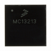
MC13213 Freescale Semiconductor, MC13213 Datasheet - Page 34

MC13213
Manufacturer Part Number
MC13213
Description
IC TXRX RF 2.4GHZ FLSH 60K 71LGA
Manufacturer
Freescale Semiconductor
Series
MC1321xr
Datasheet
1.1321XCSK-BDM.pdf
(70 pages)
Specifications of MC13213
Frequency
2.4GHz
Data Rate - Maximum
250kbps
Modulation Or Protocol
802.15.4 Zigbee
Applications
General Purpose
Power - Output
3dBm
Sensitivity
-92dBm
Voltage - Supply
1.8 V ~ 3.6 V
Current - Receiving
42mA
Current - Transmitting
35mA
Data Interface
PCB, Surface Mount
Memory Size
60kB Flash, 4kB RAM
Antenna Connector
PCB, Surface Mount
Operating Temperature
-40°C ~ 85°C
Package / Case
71-LGA
Number Of Receivers
1
Number Of Transmitters
1
Wireless Frequency
2.4 GHz to 2.48 GHz
Interface Type
SPI
Output Power
0 dBm to 2 dBm
Operating Supply Voltage
2 V to 3.4 V
Maximum Operating Temperature
+ 85 C
Mounting Style
SMD/SMT
Maximum Supply Current
42 mA
Minimum Operating Temperature
- 40 C
Protocol Supported
802.15.4
Lead Free Status / RoHS Status
Lead free / RoHS Compliant
Available stocks
Company
Part Number
Manufacturer
Quantity
Price
Company:
Part Number:
MC13213
Manufacturer:
FREESCALE Semiconductor
Quantity:
337
Part Number:
MC13213
Manufacturer:
FREESCALE
Quantity:
20 000
Company:
Part Number:
MC13213R2
Manufacturer:
BROADCOM
Quantity:
1
Part Number:
MC13213R2
Manufacturer:
FREESCALE
Quantity:
20 000
5.7.1.1
Features of the SPI module use include:
5.7.1.2
Figure 19
Data is written to the double-buffered transmitter (write to SPI1D) and gets transferred to the SPI shift
register at the start of a data transfer. After shifting in a byte of data, the data is transferred into the
double-buffered receiver where it can be read (read from SPI1D). Pin multiplexing logic controls
connections between MCU pins and the SPI module.
When the SPI is configured as a master, the clock output is routed to the SPSCK pin, the shifter output is
routed to MOSI, and the shifter input is routed from the MISO pin.
34
•
•
•
•
•
•
Used in master mode only
Programmable transmit bit rate (maximum usable rate is 8 MHz with modem)
Double-buffered transmit and receive
Serial clock phase and polarity option must be programmed to CPHA = 0 and CPOL = 0
Programmable slave select output to support modem SPI protocol
MSB-first data transfer
BUS RATE
CLOCK
is a block diagram of the SPI module. The central element of the SPI is the SPI shift register.
SPI SYSTEM
ENABLE
LSBFE
SPE
MSTR
SPI Features
SPI Module Block Diagram
CLOCK GENERATOR
SPIBR
MASTER/SLAVE
MODE SELECT
DIRECTION
SHIFT
OUT
SHIFT
Tx BUFFER (WRITE
Figure 19. Modem Dedicated SPI Block Diagram
MODE FAULT
Rx BUFFER (READ)
SPI SHIFT REGISTER
DETECTION
SHIFT
CLOCK
CLOCK
LOGIC
MODF
MC13211/212/213 Technical Data, Rev. 1.8
Rx BUFFER
FULL
SPRF
Tx BUFFER
EMPTY
SHIFT
SPTEF
SPTIE
SPIE
IN
MASTER CLOCK
SLAVE CLOCK
BIDIROE
SPC0
SSOE
MOD-
PIN CONTROL
M
S
M
S
M
S
MASTER/
SLAVE
SPI
INTERRUPT
REQUEST
SPSCK
MOSI
MISO
Connected onboard SiP
SS
MOSI
MISO
SPICLK
CE
Freescale Semiconductor
MODEM
PORT
SPI


