CYWM6934 Cypress Semiconductor Corp, CYWM6934 Datasheet - Page 5
CYWM6934
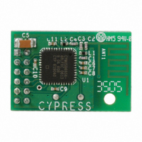
Manufacturer Part Number
CYWM6934
Description
MODULE WIRELESS USB LS
Manufacturer
Cypress Semiconductor Corp
Specifications of CYWM6934
Frequency
2.4GHz
Data Rate - Maximum
62.5kbps
Modulation Or Protocol
DSSS, GFSK
Applications
HID, PC, Peripheral Gaming Devices
Power - Output
0dBm
Sensitivity
-90dBm
Voltage - Supply
2.7 V ~ 3.6 V
Data Interface
Connector, 2 x 6 Header, 2mm Pitch
Antenna Connector
On-Board, Trace
Package / Case
Module
Wireless Frequency
2.4 GHz
Interface Type
USB
Board Size
24.38 mm x 16.25 mm x 5.3 mm
Operating Voltage
2.7 V to 3.6 V
Frequency Range
2.4GHz To 2.483GHz
Data Rate Max
62.5Kbps
Module Interface
SPI
Supply Voltage Range
2.7V To 3.6V
Supply Voltage Min
2.7V
Operating Temperature Max
70°C
Peak Reflow Compatible (260 C)
No
Features
10
Internal Oscillator Frequency
24MHz
Leaded Process Compatible
No
Sensitivity (dbm)
-90dBm
Lead Free Status / RoHS Status
Lead free / RoHS Compliant
Operating Temperature
-
Memory Size
-
Current - Transmitting
-
Current - Receiving
-
Lead Free Status / Rohs Status
Lead free / RoHS Compliant
Other names
428-1945
CYWM6934
CYWM6934


Product Labeling Requirements
European Union product labeling requirements stipulate specific
text be placed on the device containing the CYWM6934 module.
The product label must include the following text and must be
affixed to the exterior of the OEM’s product. (As shown in the
‘Correct Labeling’ section 4.1.3). This same information may be
included in the product user manual, however this is not
mandatory. Packaging and user documentation must indicate
Pin Definitions
Table 1. Pin Description Table for the CYWM6934
Document 38-16012 Rev. *B
Pin QFN
10
11
12
1
2
3
4
5
6
7
8
9
nRESET
Name
MOSI
MISO
GND
GND
VCC
SCK
nSS
nPD
IRQ
N/C
N/C
Direction
Output
Output
Input
Input
Input
Input
Input
–
–
–
–
–
Ground
Supply voltage for the entire Radio Module (2.7 V-3.6 V). It is recommended that 3.3 V be used for most
applications.
Interrupt signal from Radio Module to the MCU
Active low reset signal from MCU to Radio Module
Master out, slave in SPI signal from MCU to Radio Module
Active low slave select signal from MCU to Radio Module
SPI clock from MCU to Radio Module
Master in, slave out SPI signal from Radio Module to MCU
Ground
Active low power-down signal from MCU to Radio Module
No connect—leave open
No connect—leave open
Figure 1. CYWM6934 Header Pin-out
MOSI
GND
GND
SCK
IRQ
N/C
11
header
1
3
5
7
9
12-pin
2mm
10
12
2
4
6
8
the use restrictions of the end-product (i.e. countries disallowing
the operating frequencies of the CYWM6934).
Note:
The end-product must be labeled "CE" and to the right of the CE
mark, the label should have '!' with a circle around it. The
exclamation mark designates a non-harmonized frequency
band.
nSS
V CC
MISO
nPD
N/C
nRESET
Description
CYWM6934
Page 5 of 9
Related parts for CYWM6934
Image
Part Number
Description
Manufacturer
Datasheet
Request
R

Part Number:
Description:
Manufacturer:
Cypress Semiconductor Corp
Datasheet:
Part Number:
Description:
Manufacturer:
Cypress Semiconductor Corp
Datasheet:
Part Number:
Description:
Manufacturer:
Cypress Semiconductor Corp
Datasheet:
Part Number:
Description:
Manufacturer:
Cypress Semiconductor Corp
Datasheet:
Part Number:
Description:
Manufacturer:
Cypress Semiconductor Corp
Datasheet: