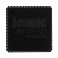
JN5139-Z01-V NXP Semiconductors, JN5139-Z01-V Datasheet - Page 2

JN5139-Z01-V
Manufacturer Part Number
JN5139-Z01-V
Description
IC MCU ZIGBEE 32BIT 2.4G 56QFN
Manufacturer
NXP Semiconductors
Series
JN5139-Z01Rxr
Specifications of JN5139-Z01-V
Frequency
2.4GHz
Modulation Or Protocol
802.15.4 Zigbee
Applications
General Purpose
Power - Output
3dBm
Sensitivity
-97dBm
Voltage - Supply
2.2 V ~ 3.6 V
Current - Receiving
34mA
Current - Transmitting
34mA
Data Interface
PCB, Surface Mount
Memory Size
96kB RAM, 192kB ROM
Antenna Connector
PCB, Surface Mount
Operating Temperature
-40°C ~ 85°C
Package / Case
56-QFN
Lead Free Status / RoHS Status
Lead free / RoHS Compliant
Data Rate - Maximum
-
Other names
616-1034-2
935293943515
JN5139-Z01-AI
JN5139-Z01-V
JN5139-Z01R1-ARV
JN5139-Z01R1V
935293943515
JN5139-Z01-AI
JN5139-Z01-V
JN5139-Z01R1-ARV
JN5139-Z01R1V
Design Flexibility
Battery Optimisation
To maximise battery life, devices support a series of power
management and sleep modes. Used effectively, these will allow a
batteries life expectancy for a typical remote sensing application, to
be of the order of a few years.
Wireless Protocol Stacks in ROM
Two standard ROM configurations are available that integrate IEEE802.15.4b and ZigBee protocol stacks. The JN5139-000
integrates IEEE802.15.4b for development of proprietary systems, and the JN5139-Z01 integrates the ZigBee protocol stack,
this supporting co-ordinator, router and end device configurations. Custom ROM masks will support the integration of user
code into ROM, attractive to higher volume applications.
Application Diagram
The JN5139 device requires a minimum of external
components to support wireless applications; a crystal,
some decoupling components and printed antenna are
all that is required for the lowest cost bill of materials and
smallest size (an external bootloader flash may be used
for optional program code storage).
Evaluation Kits
To assist users with the development of wireless sensor networks, Jennic provide a series of Evaluation Kits. These contain
everything that is needed to carry out complete development and test, and include controller and sensor boards, interface
dongle to connect with a PC and a Software Developer Kit (SDK).
The SDK provides a comprehensive suite of tools to facilitate the development of application code. The kit includes a C
compiler, graphical and text debuggers, assembler, linker and flash programmer. A set of libraries provides a simple
Application Programming Interface (API) to drive the peripherals of the controller and sensor boards.
© Jennic Ltd 2008 – www.jennic.com
Corporate Headquarters
Furnival Street
Sheffield
S1 4QT
United Kingdom
Tel
Fax
E-mail
+44 (0)114 2812655
+44 (0)114 2812951
info@jennic.com
Taiwan Sales Office
19F-1, 182, Sec.2
Tun Hwa S. Road
Taipei 106
Taiwan
Tel
Fax
E-mail
+886 2 2735 7357
+886 2 2739 5687
info@tw.jennic.com
JN5139-PB v1.22
RESET
UART 1
C10
C11
Y1
CLK O/P
Serial Port
C15
Two Wire
C8
C7
Japan Sales Office
Osakaya building 4F
1-11-8 Higashigotanda
Shinagawa-ku
Tokyo 141-0022, Japan
Tel
Fax
E-mail
VCOTUNE
VB_PROT
C9
XTALOUT
R4
Vcc
CLK_OP
RESETN
VB_SYN
XTALIN
VSSS
RXD1
VSS2
VSS3
CTS1
RTS1
TXD1
C2
C12
1
Power Saving Mode
Deep sleep
Sleep: wakeup on I/O or timer event
Sleep: wakeup on I/O or timer event and 96kB RAM retained
15
+81 3 5449 7501
+81 3 5449 0741
info@jp.jennic.com
Timers
Printed Antenna
R9
Jennic
JN513x
C13
C3
C1
Vcc
43
C4
29
UART 0
SPISEL3
SPISEL2
VB_MEM
SPISEL1
SPISEL0
MISO
MOSI
SPICLK
COMP2P
VSS1
VB_APP
COMP2M
DAC1
DAC2
United States Sales Office
1060 First Avenue, Suite 400
King of Prussia
PA 16406
USA
Tel
Fax
E-mail
C6
C5
Analogue IO
+1 610 768 8071
+1 484 971 5015
info@us.jennic.com
Optional Bootloader
SPI Selects
IC2 Serial Flash Memory
1
2
3
4
SS
SDO
WP
Vss
Flash
HOLD
CLK
Vcc
SDI
Page 2 of 2
8
7
6
5
Current
Typical
Vcc
0.2µA
1.3µA
3.3µA


