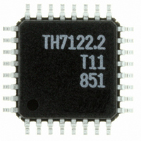
TH7122ENE Melexis Inc, TH7122ENE Datasheet - Page 5

TH7122ENE
Manufacturer Part Number
TH7122ENE
Description
IC TXRX 930MHZ FSK/FM/ASK 32LQFP
Manufacturer
Melexis Inc
Specifications of TH7122ENE
Frequency
300MHz ~ 930MHz
Data Rate - Maximum
115Kbps
Modulation Or Protocol
ASK, FM, FSK
Applications
Alarm and Security Systems, RKE, TPMS
Power - Output
-10dBm ~ 11dBm
Sensitivity
-105dBm
Voltage - Supply
2.2 V ~ 5.5 V
Current - Receiving
14mA
Current - Transmitting
23mA @ 10dBm
Data Interface
PCB, Surface Mount
Antenna Connector
PCB, Surface Mount
Operating Temperature
-40°C ~ 85°C
Package / Case
32-LQFP
Transmitting Current
12mA
Data Rate
115Kbps
Frequency Range
300MHz To 930MHz
Modulation Type
AM, FM, FSK
Sensitivity Dbm
-105dBm
Rf Ic Case Style
LQFP
No. Of Pins
32
Supply Voltage
RoHS Compliant
Output Power
10dBm
Rohs Compliant
Yes
Lead Free Status / RoHS Status
Lead free / RoHS Compliant
Memory Size
-
Lead Free Status / RoHS Status
Lead free / RoHS Compliant
Other names
TH7122.3
TH7122ENETR
TH7122ENETR
Available stocks
Company
Part Number
Manufacturer
Quantity
Price
1.4
1.5
The transceiver can operate in two different user modes. It can be used either as a 3wire-bus-controlled
programmable or as a stand-alone fixed-frequency device. After power up, the transceiver is set to Stand-
alone User Mode (SUM). In this mode, pins FS0/SDEN and FS1/LD must be connected to V
order to set the desired frequency of operation. There are 4 pre-defined frequency settings: 315MHz,
433.92MHz, 868.3MHz and 915MHz. The logic level at pin FS0/SDEN must not be changed after power up
in order to remain in fixed-frequency mode.
After the first logic level change at pin FS0/SDEN, the transceiver enters into Programmable User Mode
(PUM). In this mode, the user can set any PLL frequency or mode of operation by the SCI. In SUM pins
FS0/SDEN and FS1/LD are used to set the desired frequency, while in PUM pin FS0/SDEN is part of the
3-wire serial control interface (SCI) and pin FS1/LD is the look detector output signal of the PLL synthesizer.
A mode control logic allows several operating modes. In addition to standby, transmit and receive mode, two
idle modes can be selected to run either the reference oscillator only or the whole PLL synthesizer. The PLL
settings for the PLL idle mode are taken over from the last operating mode which can be either receive or
transmit mode.
The different operating modes can be set in SUM and PUM as well. In SUM the user can program the trans-
ceiver via control pins RE/SCLK and TE/SDTA. In PUM the register bits OPMODE are used to select the
modes of operation while pins RE/SCLK and TE/SDTA are part of the SCI.
39010 07122
Rev. 010
IN_LNA
25
26
OUT_PA
Block Diagram
User Mode Features
27
LNA
24
29
PA
ASK
PS_PA
28
30
21
TNK_LO
VCO
MIX
LO
counter
20
32
N
IF
VCC_PLL
31
Fig. 1:
1
23
LF
2
IFA
22
counter
RO
7
TH7122 block diagram
Page 5 of 44
VEE_PLL
R
10
1.5pF
RO
RO
FSK
11
MIX
3
19
IN_DEM
Demodulator
FSK
9
FSK/FM/ASK Transceiver
SW1
PKDET
12
Control Logic
13
15
6
OUT_DEM
SW2
16
200k
17
27 to 930MHz
TH7122
bias
18
OA1
OA2
SCI
EE
OUT_DTA
INT2/PDO
14
Data Sheet
or V
INT1
8
4
5
Feb/09
CC
in


