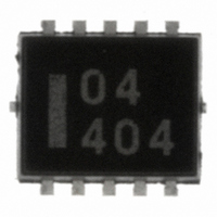
NJG1519KC1-TE3 NJR, NJG1519KC1-TE3 Datasheet

NJG1519KC1-TE3
Specifications of NJG1519KC1-TE3
Related parts for NJG1519KC1-TE3
NJG1519KC1-TE3 Summary of contents
Page 1
... SP4T SWITCH GaAs MMIC nGENERAL DESCRIPTION NJG1519KC1 is a GaAs high power SP4T switch MMIC for antenna switch of dual mode cellular phone application such as GSM/DCS1800. This switch is designed for an antenna switch between an antenna and one of two Tx ports or two Rx ports to control RF signals up to 2.5GHz. ...
Page 2
... NJG1519KC1 nABSOLUTE MAXIMUM RATINGS PARAMETER SYMBOL RF Input Power Operating Voltage Power Dissipation Operating Temp. Storage Tempe. nELECTRICAL CHARACTERISTICS PARAMETER SYMBOL Control Voltage (Low) V Control Voltage (High) V Control Current Insertion loss 1 LOSS1 Insertion loss 2 LOSS2 Isolation 1 Isolation 2 Pin at 0.2dB P Compression point VSWR ...
Page 3
... Control port4. Please connect bypass capacitor (10pF) between this terminal and GND close to this IC. RF port. This terminal is connected under the condition of 9pin-V (+2.5~+6.5V 7pin-V CTL( cut capacitor 56pF is reguired at this terminal to block DC voltage of inner circuit. NJG1519KC1 (-0.2~+0.2V). CTL(L) (-0.2~+0.2V). CTL(L) (-0.2~+0.2V). CTL(L) (-0.2~+0.2V). ...
Page 4
... NJG1519KC1 nELECTRICAL CHARACTERISTICS (f=100MHz~3.0GHz, with application circuit, losses of external circuit are excluded) PC-P1 Insertion Loss vs. Frequency ( V =3.0V, V CTL(H) 0.0 -0.5 -1.0 -1.5 -2.0 0.0 0.5 1.0 1.5 Frequency (GHz) VSWR(P1) vs. Frequency (PC-P1 ON, V =3.0V ,V CTL(H) 2.0 1.8 1.6 1.4 1.2 1.0 ...
Page 5
... CTL( -10 -15 -20 -25 -30 -35 -40 -45 2.0 2.5 3.0 0.0 NJG1519KC1 PC-P2 Isolation vs. Frequency (PC-P3 ON, V =3.0V ,V =0V) CTL(H) CTL(L) 0.5 1.0 1.5 2.0 2.5 Frequency (GHz) PC-P4 Isolation vs. Frequency (PC-P1 ON, V =3.0V ,V =0V) CTL(H) CTL(L) 0.5 1.0 1 ...
Page 6
... NJG1519KC1 nELECTRICAL CHARACTERISTICS (f=900MHz, with application circuit, losses of PCB, connector and DC blocking capacitor are excluded) Output Power,Control Current vs. Input Power ( PC-P1 ON, f=900MHz ) 38 VCTL=2.5V 36 VCTL=2.7V VCTL=3. Input Power (dBm) Insertion Loss vs. Input Power ( PC-P1 ON, f=900MHz ) 0.0 VCTL=2.5V VCTL=2.7V VCTL=3.0V -0.5 -1.0 -1.5 -2 ...
Page 7
... Input Power (dBm) -10 -15 -20 -25 - Output Power,Control Current vs. Input Power 180 38 160 36 140 34 120 32 100 NJG1519KC1 PC-P1 Isolation vs. Input Power ( PC- f=900MHz ) VCTL=3.0V VCTL=3.6V VCTL=4.8V VCTL=6. Input Power (dBm) ( PC-P1 ON, f=1.9GHz ) VCTL=3.0V VCTL=3.0V VCTL=3.6V VCTL=3.6V VCTL=4.8V VCTL=4.8V VCTL=6.5V VCTL=6. Input Power (dBm) 36 ...
Page 8
... NJG1519KC1 nELECTRICAL CHARACTERISTICS (f=1.9GHz, with application circuit, losses of PCB, connector and DC blocking capacitor are excluded) Insertion Loss vs. Input Power ( PC-P1 ON, f=1.9GHz ) 0.0 VCTL=2.5V VCTL=2.7V VCTL=3.0V -0.5 -1.0 -1.5 -2 Input Power (dBm) PC-P1 Isolation vs. Input Power ( PC-P4 ON, f=1.9GHz ) 0 VCTL=2.5V VCTL=2.7V VCTL=3.0V -5 -10 ...
Page 9
... NJG1519KC1 2nd Harmonics vs. Input Power (PC-P1 ON ,f=1.9GHz) VCTL=2.5V VCTL=3.6V VCTL=2.7V VCTL=4.8V VCTL=3.0V VCTL=6.5V Input 2fo Level=-90dBc Input Power (dBm) 3rd Harmonics vs. Input Power (PC-P1 ON ,f=1.9GHz) VCTL=2.5V VCTL=2.7V VCTL=3.0V VCTL=3.6V VCTL=4.8V VCTL=6 ...
Page 10
... NJG1519KC1 nELECTRICAL CHARACTERISTICS 1.2V 200mV /div trlg’d -800mV -94ns - 10 - (with application circuit) Switching speed (V =3.0V, V =0V) CTL1 CTL2 80nsec 50ns/div 406ns ...
Page 11
... Insertion Loss vs. Ambient Temperature 0.0 -0.5 -1.0 -1.5 -2.0 50 100 - Control Current vs. Ambient Temperature 120 100 100 - NJG1519KC1 ( PC-P1 ON ,f=1.9GHz ,Pin=32dBm ) VCTL=2.5V VCTL=2.7V VCTL=3.0V VCTL=3.6V VCTL=4.8V VCTL=6. Ambient Temperature ( C) ( PC- f=1.9GHz ,Pin=32dBm ) VCTL=2.5V VCTL=2.7V VCTL=3.0V VCTL=3.6V VCTL=4.8V VCTL=6. Ambient Temperature ( C) ...
Page 12
... NJG1519KC1 nTEMPERATURE CHARACTERISTICS PC-P1 Isolation vs. Ambient Temperature ( PC-P2 ON ,f=900MHz ,Pin=34dBm ) 0 VCTL=2.5V -5 VCTL=2.7V VCTL=3.0V VCTL=3.6V -10 VCTL=4.8V VCTL=6.5V -15 -20 -25 -30 -35 -40 -50 0 Ambient Temperature ( PC-P3 Isolation vs. Ambient Temperature ( PC-P4 ON ,f=900MHz ,Pin=34dBm ) 0 VCTL=2.5V -5 VCTL=2.7V VCTL=3.0V VCTL=3.6V -10 VCTL=4.8V VCTL=6.5V -15 -20 -25 -30 -35 -40 -50 0 Ambient Temperature ( ...
Page 13
... C) PC-P4 Isolation vs. Ambient Temperature 0 -5 -10 -15 -20 -25 -30 -35 -40 50 100 - NJG1519KC1 ( PC-P3 ON ,f=1.9GHz ,Pin=32dBm ) VCTL=2.5V VCTL=2.7V VCTL=3.0V VCTL=3.6V VCTL=4.8V VCTL=6. Ambient Temperature ( C) ( PC-P1 ON ,f=1.9GHz ,Pin=32dBm ) VCTL=2.5V VCTL=2.7V VCTL=3.0V VCTL=3.6V VCTL=4.8V VCTL=6. Ambient Temperature ( C) 100 100 - 13 - ...
Page 14
... NJG1519KC1 nTEMPERATURE CHARACTERISTICS 2nd Harmonics vs. Ambient Temperature ( PC-P1 ON ,f=900MHz ,Pin=34dBm ) -45 VCTL=2.5V VCTL=3.6V VCTL=2.7V VCTL=4.8V -50 VCTL=3.0V VCTL=6.5V -55 -60 -65 -70 Input 2fo Level=-90dBc -75 -50 0 Ambient Temperature ( 3rd Harmonics vs. Ambient Temperature ( PC-P1 ON,f=900MHz ,Pin=34dBm ) -20 VCTL=2.5V VCTL=3.6V VCTL=2.7V VCTL=4.8V -30 VCTL=3.0V VCTL=6.5V -40 -50 -60 -70 Input 3fo Level=-115dBc ...
Page 15
... To avoid degradation of isolation or high power characteristics, please layout ground pattern right under this IC NJG1519KC1 P4 PCB: FR-4, t=0.5mm Microstrip Line Width: 1mm (Z PCB Size: 26x26mm nPARTS LIST VCTL4 nCircuit losses including losses of VCTL3 capacitors and connectors P3 NJG1519KC1 P4 C4 56pF 10 VCTL4 C9 10pF 9 C5 56pF 10pF VCTL3 56pF =50 ) ...
Page 16
... NJG1519KC1 nPACKAGE OUTLINE (FLP10-C1) 3.0± 0 0.5 0.5 +0.1 0.2 -0.05 Cautions on us ing this product This product contains Gallium-Arsenide (GaAs) which is a harmful material. Do NOT eat or put into mouth. Do NOT dispose in fire or break up this product. Do NOT chemically make gas or powder with this product. ...


