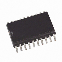
ATA5743P6-TKSY Atmel, ATA5743P6-TKSY Datasheet - Page 21

ATA5743P6-TKSY
Manufacturer Part Number
ATA5743P6-TKSY
Description
IC RCVR ASK/FSK 600KHZ 20SSOP
Manufacturer
Atmel
Datasheet
1.ATA5743P3-TGQY.pdf
(43 pages)
Specifications of ATA5743P6-TKSY
Frequency
300MHz ~ 450MHz
Sensitivity
-110dBm
Data Rate - Maximum
10 kBaud
Modulation Or Protocol
ASK, FSK
Applications
RKE, Telemetering, Security Technology
Current - Receiving
7.5mA
Data Interface
PCB, Surface Mount
Antenna Connector
PCB, Surface Mount
Voltage - Supply
4.5 V ~ 5.5 V
Operating Temperature
-40°C ~ 105°C
Package / Case
20-SOIC (0.300", 7.50mm Width)
Operating Frequency (max)
450000kHz
Operating Temperature (min)
-40C
Operating Temperature (max)
105C
Operating Temperature Classification
Industrial
Product Depth (mm)
4.4mm
Operating Supply Voltage (min)
4.5V
Operating Supply Voltage (typ)
5V
Operating Supply Voltage (max)
5.5V
Lead Free Status / RoHS Status
Lead free / RoHS Compliant
Features
-
Memory Size
-
Lead Free Status / Rohs Status
Compliant
Figure 6-16. Data Clock Disappears Because of a Logical Error
Figure 6-17. Output of the Data Clock After a Successful Bit Check
4839B–RKE–08/05
Dem_out
Data_out (DATA)
DATA_CLK
Dem_out
Data_out (DATA)
DATA_CLK
The delay of the data clock is calculated as follows:
t
t
depends on the capacitive load C
falling edge, t
Figure 6-19 on page 22
level of Data_Out, the data clock is issued after an additional delay t
Note that the capacitive load at pin DATA is limited. If the maximum tolerated capacitive load at
pin DATA is exceeded, the data clock disappears (see section
Delay
Delay1
= t
is the delay between the internal signals Data_Out and Data_In. For the rising edge, t
Delay1
1
1
Receiving mode,
bit check active
Bit check ok
+ t
Delay1
1
1
Delay2
depends additionally on the external voltage V
Receiving mode,
data clock control
logic active
1
1
and
0
1
Figure 6-26 on page
L
1
1
at pin DATA and the external pull-up resistor R
Data
Start bit
Data
1
0
Logical error (Manchester code violation)
Receiving mode,
data clock control
logic active
?
1
29). When the level of Data_In is equal to the
0
1
Receiving mode,
bit check aktive
0
0
“Data Interface” on page
X
(see
1
1
Delay2
Figure 6-18 on page
.
0
0
ATA5743
pup
. For the
29).
Delay1
22,
21


