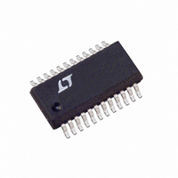
LT5500EGN Linear Technology, LT5500EGN Datasheet - Page 6

LT5500EGN
Manufacturer Part Number
LT5500EGN
Description
IC RECEIVER FRONT END 24-SSOP
Manufacturer
Linear Technology
Datasheet
1.LT5500EGN.pdf
(12 pages)
Specifications of LT5500EGN
Frequency
1.8GHz ~ 2.7GHz
Applications
HS Wireless LAN, Wireless Local Loop
Current - Receiving
23mA
Data Interface
PCB, Surface Mount
Antenna Connector
PCB, Surface Mount
Voltage - Supply
1.8 V ~ 5.25 V
Operating Temperature
-40°C ~ 85°C
Package / Case
24-SSOP
Pin Count
24
Screening Level
Industrial
Lead Free Status / RoHS Status
Contains lead / RoHS non-compliant
Features
-
Sensitivity
-
Memory Size
-
Data Rate - Maximum
-
Modulation Or Protocol
-
Lead Free Status / Rohs Status
Not Compliant
Available stocks
Company
Part Number
Manufacturer
Quantity
Price
Company:
Part Number:
LT5500EGN
Manufacturer:
LT
Quantity:
5 549
Part Number:
LT5500EGN
Manufacturer:
LINEAR/凌特
Quantity:
20 000
Part Number:
LT5500EGN#PBF
Manufacturer:
LINEAR/凌特
Quantity:
20 000
Part Number:
LT5500EGN#TRPBF
Manufacturer:
LINEAR/凌特
Quantity:
20 000
PIN
LT5500
EN (Pin 1): Enable Pin. A voltage less than 0.3V (Logic Low)
disables the part. An input greater than 1.35V (Logic High)
enables the part. This pin should be bypassed to ground with
a 100pF capacitor. To shut down the part, this pin and GS
(Pin 24) must be logic low. Voltage on this pin should not
exceed V
V
for recommended power supply bypassing.
LNA_IN (Pin 3): LNA Input Pin. The LT5500 has better
than 10dB input return loss from 1.8GHz to 2.7GHz. This
pin is internally biased to 0.8V and must be AC coupled.
GND (Pin 4, 11, 14, 16, 20, 23): Ground Pins. These pins
should be connected directly to ground.
LNA_GND (Pins 5, 6, 7, 8): LNA Ground Pins. These pins
control the gain of the LNA. At higher frequencies, these
pins must be connected directly to ground to maximize the
gain.
MIX_GND (Pin 10): Mixer Ground Pin. To optimize the
performance of the mixer, a 4.7nH inductor to ground is
required for this pin.
IF
Output Pins. These pins must be inductively tied to V
6
CC
+
U
, IF
(Pins 2, 9, 17, 21): Power Supply Pins. See Figure 6
FUNCTIONS
–
(Pins 12, 13): Intermediate Frequency (IF) Mixer
CC
U
nor fall below ground.
U
CC
.
The output can be taken differentially or transformed into
a single ended output, depending on user preference and
performance requirements.
MIX_IN (Pin 15): Mixer RF Input. This pin is internally
biased to 0.83V and must be AC coupled. An external
matching network is necessary to match to a 50Ω system.
LO
used to provide the LO drive to the mixer. The signal can
be provided either single ended or differentially. These
pins are internally biased to V
coupled.
LNA_OUT (Pin 22): The Output Pin for the LNA. An
external matching network is necessary to match to a 50Ω
system. This pin must be DC coupled to the power supply.
GS (Pin 24): Gain Select Pin. This pin is used to select
between high gain and low gain modes. High gain mode is
selected when an input voltage greater than 1.35V (Logic
High) is applied to this pin. Low gain mode is selected
when the applied voltage is less than 0.3V (Logic Low).
This pin should be bypassed to ground with a 100pF
capacitor. To shut down the part, this pin must be logic
low. Voltage on this pin should not exceed V
below ground.
+
, LO
–
(Pins 18, 19): LO Input Pins. These pins are
CC
– 0.2V and must be AC
CC
nor fall
5500f


