RXM-900-HP3-PPO_ Linx Technologies Inc, RXM-900-HP3-PPO_ Datasheet
RXM-900-HP3-PPO_
Specifications of RXM-900-HP3-PPO_
Available stocks


Related parts for RXM-900-HP3-PPO_


RXM-900-HP3-PPO_ Summary of contents
Page 1
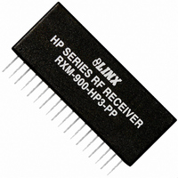
... Direct serial interface MDEV-900-HP3-SPS-USB Pinned and SMD packages MDEV-900-HP3-SPS-RS232 Wide temperature range Receivers are supplied in tubes of 10 pcs. (-30°C to +85°C) 1.940" HP SERIES RF RECEIVER 0.780" RXM-900-HP3-SP* LOT 10000 Pin Spacing: 0.1" 0.236" SIP Style 1.950" HP SERIES RF RECEIVER 0.750" RXM-900-HP3-SP* LOT 10000 0.190" ...
Page 2
ELECTRICAL SPECIFICATIONS Parameter Designation Min. POWER SUPPLY Operating Voltage V 2.8 CC Supply Current I 16.0 CC Power-Down Current I – PDN RECEIVE SECTION Receive Frequency Range F 902.62 C Center Frequency Accuracy -50 Channel Spacing – – First IF ...
Page 3
PIN ASSIGNMENTS Pinned Receiver Figure 7: HP3 Series Receiver Pinout Pin # Name Description 1 ANT 50-ohm RF Input 2-8 GND Analog Ground Connection 10 CS0 Channel Select 0 Channel Select 1 / Serial Select Clock. Channel ...
Page 4
THEORY OF OPERATION The HP3 is a high-performance multi-channel, dual-conversion superhet receiver capable of recovering both analog (FM) and digital (FSK) information from a matching HP Series transmitter FSK modulation offers significant advantages over AM or OOK modulation ...
Page 5
THE DATA OUTPUT The DATA line outputs recovered digital data open collector output with an internal 4.7kΩ pull-up. When an RF transmission is not present, or when the received signal strength is too low to ensure proper ...
Page 6
CHANNEL SELECTION Parallel Selection CS2 0 All HP3 receiver models feature eight 0 parallel selectable channels. Parallel 0 0 Mode is selected by grounding the 1 MODE line. In this mode, channel 1 selection is determined by the logic 1 ...
Page 7
PROTOCOL GUIDELINES While many RF solutions impose data formatting and balancing requirements, Linx RF modules do not encode or packetize the signal content in any manner. The received signal will be affected by such factors as noise, edge jitter, and ...
Page 8
BOARD LAYOUT GUIDELINES If you are at all familiar with RF devices, you may be concerned about specialized board layout requirements. Fortunately, because of the care taken by Linx in designing the modules, integrating them is very straightforward. Despite this ...
Page 9
PAD LAYOUT The following pad layout diagram is designed to facilitate both hand and automated assembly. Pinned Receiver 0.090 0.060 0.100 0.060 0.030 Dia. Finished Figure 18: Recommended PCB Layout PRODUCTION GUIDELINES The modules are housed in a hybrid SMD ...
Page 10
ANTENNA CONSIDERATIONS The choice of antennas is a critical and often overlooked design consideration. The range, performance, and legality link are critically dependent upon the antenna. While adequate antenna performance can often be obtained by trial and ...
Page 11
COMMON ANTENNA STYLES There are literally hundreds of antenna styles and variations that can be employed with Linx RF modules. Following is a brief discussion of the styles most commonly utilized. Additional antenna information can be found in Linx Application ...
Page 12
LEGAL CONSIDERATIONS NOTE: Linx RF modules are designed as component devices that require external components to function. The modules are intended to allow for full Part 15 compliance; however, they are not approved by the FCC or any other agency ...
Page 13
WIRELESS MADE SIMPLE U.S. CORPORATE HEADQUARTERS LINX TECHNOLOGIES, INC. 159 ORT LANE MERLIN, OR 97532 PHONE: (541) 471-6256 FAX: (541) 471-6251 www.linxtechnologies.com Disclaimer Linx Technologies is continually striving to improve the quality and function of its products. For this ...