ATA3741P2-TGQY Atmel, ATA3741P2-TGQY Datasheet - Page 21

ATA3741P2-TGQY
Manufacturer Part Number
ATA3741P2-TGQY
Description
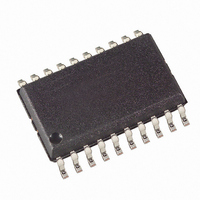
IC UHF ASK/FSK RECEIVER 20SOIC
Manufacturer
Atmel
Datasheet
1.ATA3741P2-TGSY.pdf
(31 pages)
Specifications of ATA3741P2-TGQY
Frequency
300MHz ~ 450MHz
Sensitivity
-108dBm
Data Rate - Maximum
10 kBaud
Modulation Or Protocol
ASK, FSK
Applications
RKE, TPM, Security Systems
Current - Receiving
7mA
Data Interface
PCB, Surface Mount
Antenna Connector
PCB, Surface Mount
Voltage - Supply
4.5 V ~ 5.5 V
Operating Temperature
-40°C ~ 105°C
Package / Case
20-SOIC (0.300", 7.50mm Width)
Lead Free Status / RoHS Status
Lead free / RoHS Compliant
Features
-
Memory Size
-
Other names
ATA3741P2-TGQYTR
Available stocks
Company
Part Number
Manufacturer
Quantity
Price
Company:
Part Number:
ATA3741P2-TGQY
Manufacturer:
Atmel
Quantity:
1 896
Company:
Part Number:
ATA3741P2-TGQY
Manufacturer:
ATMEL
Quantity:
18 862
Figure 5-13. Generation of the Power-on Reset
Figure 5-14. Timing of the Register Programming
5.5.2
4899B–RKE–10/06
POR
DATA (ATA3741)
Out1
(microcontroller)
DATA (ATA3741)
VS
Serial bi-directional
data line
Programming the Configuration Register
X
Receiver
on
X
X
To indicate that condition, the receiver displays a reset marker (RM) at pin DATA after a reset.
The RM is represented by the fixed frequency f
an “L” pulse t1 at pin DATA. The RM implies the following characteristics:
By means of that mechanism, the receiver cannot lose its register information without communi-
cating that condition via the reset marker RM.
The configuration registers are programmed serially via the bi-directional data line as shown in
Figure 5-14
• f
• If the receiver is set back to polling mode via pin DATA, RM cannot be canceled by accident if
misinterpreted by the connected microcontroller.
t1 is applied according to the proposal in Section
on page
RM
t1
is lower than the lowest feasible frequency of a data signal. By this means, RM cannot be
t
Rst
21.
and
t2
Figure 5-15 on page
t3
(Start bit)
Bit 1
("0")
t4
t6
t5
t7
V
ThReset
(Register select)
Bit 2
("1)
Programming Frame
22.
RM
at a 50% duty cycle. RM can be canceled via
(Poll8)
Bit 13
“Programming the Configuration Register”
("0")
1/f
RM
(Poll8R)
Bit 14
("1")
t8
t9
T
ATA3741
Sleep
Startup
mode
X
X
21


