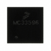
MC33596FCE Freescale Semiconductor, MC33596FCE Datasheet - Page 36

MC33596FCE
Manufacturer Part Number
MC33596FCE
Description
IC RECEIVER UHF PLL TUNED 32-QFN
Manufacturer
Freescale Semiconductor
Type
Receiverr
Datasheet
1.MC33596FCAE.pdf
(70 pages)
Specifications of MC33596FCE
Frequency
304, 315, 426, 434, 868 & 915MHz
Sensitivity
-104dBm
Data Rate - Maximum
22.4 kBaud
Modulation Or Protocol
FSK, OOK
Applications
General Data Transfer
Current - Receiving
10.3mA
Data Interface
PCB, Surface Mount
Antenna Connector
PCB, Surface Mount
Voltage - Supply
2.7 V ~ 3.6 V, 4.5 V ~ 5.5 V
Operating Temperature
-40°C ~ 85°C
Package / Case
32-QFN
Operating Frequency
915 MHz
Operating Supply Voltage
3.3 V or 5 V
Maximum Operating Temperature
+ 85 C
Minimum Operating Temperature
- 40 C
Mounting Style
SMD/SMT
Lead Free Status / RoHS Status
Request inventory verification / Request inventory verification
Features
-
Memory Size
-
Lead Free Status / Rohs Status
Lead free / RoHS Compliant
Register Description
If the data manager is disabled, the incoming signal data rate must be lower than or equal to the data
manager maximum data rate.
TRXE (Receiver Enable) enables the whole receiver. This bit must be set to high level if MCU wakes the
MC33956 to enter receive mode.
DME (Data Manager Enable) enables the data manager.
SOE (Strobe Oscillator Enable) enables the strobe oscillator.
Figure 26
OLS (Out of Lock Status) indicates the current status of the PLL.
LVDS (Low Voltage Detection Status) indicates that a low voltage event has occurred when LVDE = 1.
This bit is read-only and is cleared after a read access.
ILA[1:0] (Input Level Attenuation) define the RF input level attenuation.
36
Reset Value
Bit Name
•
•
Access
Low-pass average filter generating the data slicer reference, if DSREF is set
Data manager
0 = standby mode
1 = other modes can be activated
0 = disabled
1 = enabled
0 = disabled
1 = enabled
0 = The PLL is in lock-in range
1 = The PLL is out of lock-in range
0 = No low voltage detected
1 = Low voltage detected
describes configuration register 3, CONFIG3.
DR1
0
0
1
1
AFF1
Bit 7
R/W
DR0
0
0
1
0
1
AFF0
Cut-off Frequency
Bit 6
R/W
0
Table 10. Base Band Parameter Configuration
Data Filter
12 kHz
24 kHz
48 kHz
6 kHz
Bit 5
OLS
Figure 26. CONFIG3 Register
R
1
MC33596 Data Sheet, Rev. 4
LVDS
Bit 4
R
1
Cut-off Frequency
Average Filter
0.5 kHz
1 kHz
2 kHz
4 kHz
Bit 3
ILA1
R/W
0
Bit 2
ILA0
R/W
0
Data Rate Range
Data Manager
16–22.4 kBd
8–10.6 kBd
2–2.8 kBd
4–5.6 kBd
Bit 1
—
—
0
Freescale Semiconductor
Bit 0
—
—
0
Addr
$02


