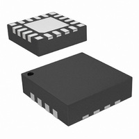
SI4312-B10-GM Silicon Laboratories Inc, SI4312-B10-GM Datasheet - Page 6

SI4312-B10-GM
Manufacturer Part Number
SI4312-B10-GM
Description
IC RX OOK 315/434MHZ 20VQFN
Manufacturer
Silicon Laboratories Inc
Series
EZRadio®r
Type
ISM Receiverr
Specifications of SI4312-B10-GM
Package / Case
20-VQFN
Frequency
315MHz, 434MHz
Sensitivity
-110dBm
Data Rate - Maximum
10 kBaud
Modulation Or Protocol
OOK
Applications
Garage Openers, RKE, Security Alarms
Data Interface
PCB, Surface Mount
Antenna Connector
PCB, Surface Mount
Voltage - Supply
2.7 V ~ 3.6 V
Operating Temperature
-40°C ~ 85°C
Operating Frequency
315 MHz to 434 MHz
Operating Supply Voltage
2.7 V to 3.6 V
Maximum Operating Temperature
+ 95 C
Minimum Operating Temperature
- 45 C
Mounting Style
SMD/SMT
Supply Current
20 mA
Lead Free Status / RoHS Status
Lead free / RoHS Compliant
Features
-
Memory Size
-
Current - Receiving
-
Lead Free Status / Rohs Status
Lead free / RoHS Compliant
Other names
336-1977-5
Table 5. Si4312 Receiver Characteristics
(T
Si4312
6
Parameter
Sensitivity @ BER = 10
Data Rate
Adjacent Channel Rejection
±200 kHz
Alternate Channel Rejection
±400 kHz
Image Rejection, IF = 128 kHz
Blocking
Maximum RF Input Power
Input IP3
LNA Input Capacitance
Receiver Channel Bandwidth
RX Boot Time
Notes:
Table 6. Crystal Characteristics
(V
Parameter
Crystal Oscillator Frequency
Crystal ESR
XTL1, XTL2 Input Capacitance
A
DD
= 25 °C, V
1. 1.0 kbps, Manchester encoded, RATIO = 0, TH[1:0] = 00, xtal = ±20 ppm.
2. Guaranteed by characterization.
3. Guaranteed by design.
4. The frequency scanning (see section “3.6. Frequency Scanning”) extends this to 420 kHz.
= 3.3 V, T
1,2
3
1,2
3
(Note 1)
DD
A
3
= 25 °C)
= 3.3 V, R
3
–3 (Note 1)
s
= 50 Ω, F
1,2
4
1,2
RF
= 433.92 MHz unless otherwise noted)
Symbol
Symbol
Desired signal is 3 dB above sensitivity
Desired signal is 3 dB above sensitivity
desired signal is 3 dB above sensitivity,
interferer level in dB when BER = 10
interferer level in dB when BER = 10
difference between desired signal and
difference between desired signal and
is at ±200 kHz, rejection measured as
is at ±400 kHz, rejection measured as
(BER = 10
(BER = 10
CW interference levels are increased
3 dB above sensitivity, CW interferer
±10 MHz, 1.0 kbps, desired signal is
3 dB above sensitivity, CW interferer
±2 MHz, 1.0 kbps, desired signal is
| f
level is increased until BER = 10
level is increased until BER = 10
2
1.0 kbps, 433.92 MHz
– f
Test Condition
1.0 kbps, 315 MHz
Rev. 0.5
10 kbps, 315 MHz
1
10 kbps, 433.92 MHz
| = 5 MHz, high gain mode,
until BER = 10
–3
–3
Test Condition
), unmodulated interferer
), unmodulated interferer
From reset
NRZ
–3
(Note2)
(Note2)
(Note2)
Min
—
—
—
–3
–3
–3
–3
Typ
16
—
11
TBD
TBD
Min
—
—
—
—
—
—
—
—
—
—
—
—
—
–103
–106
–101
–110
Typ
–10
160
500
35
55
23
65
70
—
8
7
Max
100
—
—
Max Unit
—
—
—
10
—
—
—
—
—
—
—
—
—
—
—
MHz
Unit
pF
dBm
dBm
dBm
dBm
kbps
dBm
dBm
kHz
ms
dB
dB
dB
dB
dB
pF


