MICRF213AYQS Micrel Inc, MICRF213AYQS Datasheet - Page 11

MICRF213AYQS
Manufacturer Part Number
MICRF213AYQS
Description
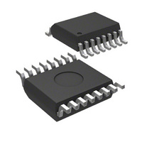
IC RX 3.3V 300-350 MHZ 16-QSOP
Manufacturer
Micrel Inc
Datasheet
1.MICRF213AYQS.pdf
(16 pages)
Specifications of MICRF213AYQS
Operating Temperature
-40°C ~ 105°C
Frequency
300MHz ~ 350MHz
Sensitivity
-110dBm
Data Rate - Maximum
7.2 kbps
Modulation Or Protocol
AM, OOK
Applications
ISM, Garage Door Openers, RKE
Current - Receiving
3.9mA
Data Interface
PCB, Surface Mount
Antenna Connector
PCB, Surface Mount
Voltage - Supply
3 V ~ 3.6 V
Package / Case
16-QSOP
Receiving Current
3.9mA
Data Rate
7.2Kbps
Modulation Type
ASK, OOK
Frequency Range
300MHz To 350MHz
Rf Ic Case Style
QSOP
No. Of Pins
16
Supply Voltage Range
3V To 3.6V
Sensitivity Dbm
-110dBm
Rohs Compliant
Yes
Operating Temperature (min)
-40C
Operating Temperature (max)
105C
Operating Temperature Classification
Industrial
Operating Supply Voltage (typ)
3.3V
Operating Supply Voltage (max)
3.6V
Lead Free Status / RoHS Status
Lead free / RoHS Compliant
Features
-
Memory Size
-
Lead Free Status / Rohs Status
Compliant
Other names
576-1649-5
Available stocks
Company
Part Number
Manufacturer
Quantity
Price
Company:
Part Number:
MICRF213AYQS
Manufacturer:
MICREL
Quantity:
600
Part Number:
MICRF213AYQS
Manufacturer:
MICR
Quantity:
20 000
For best results, the values should always be
optimized for the data pattern used. As the baud rate
increases, the capacitor values decrease. Table 9
shows suggested values for Manchester Encoded
data at 50% duty cycle.
JP3 is a jumper used to configure the digital squelch
function. When it is high, there is no squelch applied
to the digital circuits and the DO (data out) pin yields a
hash signal. When the pin is low, the DO pin activity is
considerably reduced. It will have more or less than
shown in the figure below depending upon the outside
band noise. The penalty for using squelch is a delay in
obtaining a good signal in the DO pin. That is, it takes
longer for the data to show up. The delay is
dependent upon many factors such as RF signal
intensity, data profile, data rate, Cth and Cagc
capacitor values, and outside band noise. See Figure
8 and 9.
Micrel, Inc.
May 2007
SEL0
Open
Open
Short
Short
Figure 8. Data Out Pin with No Squelch (SQ = 1)
JP1
Table 9. Suggested Cth and Cagc Values
SEL1
Short
Short
Open
Open
JP2
Demod.
(hertz)
1400
2800
5300
9700
BW
100nF
47nF
22nF
10nF
Cth
0.47uF
4.7uF
2.2uF
Cagc
1uF
DO Pin
11
Other components used include: C5, which is a
decoupling capacitor for the Vdd line; R4 reserved for
future use and not needed for the evaluation board;
R3 for the shutdown pin (SHDN = 0, device is
operation), which can be removed if that pin is
connected to a microcontroller or an external switch;
and R1 and R2 which form a voltage divider for the
AGC pin. One can force a voltage in this AGC pin to
purposely decrease the device sensitivity. Special
care is needed when doing this operation, as an
external control of the AGC voltage may vary from lot
to lot and may not work the same in several devices.
Three other pins need to be discussed as well. They
are the DO, RSSI, and shut down pins. The DO pin
has a driving capability of 0.4mA. This is good enough
for most of the logic families ICs in the market today.
The RSSI pin provides a transfer function of the RF
signal intensity vs. voltage. It is very useful to
determine the signal to noise ratio of the RF link,
crude range estimate from the transmitter source and
AM demodulation, which requires a low Cagc
capacitor value.
The shut down pin (SHDN) is useful to save energy.
Making its level close to Vdd (SHDN = 1), the device
is then not in operation. Its DC current consumption is
less than 1µA (do not forget to remove R3). When
toggling from high to low, there will be a time required
for the device to come to steady state mode, and a
time for data to show up in the DO pin. This time will
be dependent upon many things such as temperature,
crystal used, and if the there is an external oscillator
with faster startup time. Crystal vendors suggest that
the data will show up in the DO pin around 1msec
time, and 2msec over the temperature range of the
device. See Figure 10.
Figure 9. Data Out Pin with Squelch (SQ = 0)
M9999-052307-A
(408) 944-0800
MICRF213
DO Pin


