MLX71121KLQ Melexis Inc, MLX71121KLQ Datasheet
MLX71121KLQ
Specifications of MLX71121KLQ
Available stocks


Related parts for MLX71121KLQ


MLX71121KLQ Summary of contents
Page 1
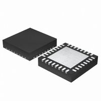
... Quad Flat No-Lead Package (QFN) Ordering Information Part Number Temperature Code MLX71121 C (-10 ° °C) Application Examples General digital and analog RF receivers at 300 to 930MHz Automatic meter reading (AMR) Consumer remote controls Low power telemetry systems Alarm and security systems Garage and gate controls ...
Page 2
Document Content 1 Theory of Operation ...................................................................................................4 1.1 General ............................................................................................................................. 4 1.2 Technical Data Overview.................................................................................................. 4 1.3 Block Diagram .................................................................................................................. 5 1.4 Operating Modes .............................................................................................................. 6 1.5 LNA Selection................................................................................................................... 6 1.6 Mixer Section.................................................................................................................... 7 1.7 IF Filter ............................................................................................................................. 7 1.8 ...
Page 3
Package Description ................................................................................................26 6.1 Soldering Information ..................................................................................................... 26 7 Reliability Information .............................................................................................27 8 ESD Precautions ......................................................................................................27 9 Disclaimer .................................................................................................................28 39010 71121 Rev. 009 FSK/FM/ASK Receiver Page MLX71121 300 to 930MHz Data Sheet Oct/10 ...
Page 4
Theory of Operation 1.1 General The MLX71121 receiver architecture is based on a double-conversion super-heterodyne approach. The two LO signals are derived from an on-chip integer-N PLL frequency synthesizer. The PLL reference frequency is derived from a crystal (XTAL). ...
Page 5
Block Diagram VEE 2 LNAI1 LNA1 1 MIX1 LNASEL 32 LO1 LNAI2 LNA2 8 VEE 7 SEQ RFSEL 31 BIAS TEST 26 30 The MLX71121 receiver IC consists of the following building blocks: • PLL ...
Page 6
Operating Modes The receiver offers two operating modes selectable by setting the corresponding logic level at pin ENRX. ENRX 0 1 Note: ENRX is pulled down internally. The receiver’s start-up procedure is controlled by a sequencer circuit. It performs ...
Page 7
Mixer Section The mixer section consists of two mixers. Both are double-balanced mixers. The second mixer is built as an image rejection mixer. The first mixer’s inputs (MIXP and MIXN) are functionally the same. For single-ended drive, the unused ...
Page 8
Reference Oscillator A Colpitts crystal oscillator with integrated functional capacitors is used as the reference oscillator (RO) of the PLL synthesizer. The equivalent input capacitance CRO offered to the crystal at pin ROI is about 18pF. The crystal oscillator features ...
Page 9
Baseband Data Path The baseband data path can be divided into a data filter section and a data slicer section. MODSEL DF1 ASK 100k 100k FSK SW1 PKDET+ 100k SLCSEL PKDET _ OA2 The data filter input is either ...
Page 10
Data Filter The data filter is formed by the operational amplifier OA1, two internal 100kΩ resistors and two external ca- pacitors implemented higher frequencies and therefore leads to an increased sensitivity. CF1 DF1 100k ...
Page 11
Averaging Detection Mode The simplest configuration is the averaging or RC inte- gration method. Here an on-chip 100kΩ resistor to- gether with an external slicer capacitor (CSL) are form- ing an RC low-pass filter. This way the threshold voltage ...
Page 12
Noise Cancellation Filter and Data Output The data output pin DTAO delivers the demodulated data signal which can be further processed by a noise cancellation filter (NCF). The NCF can be disabled if pin CINT is connected to ground. ...
Page 13
Functional Description 2.1 Frequency Planning Because of the double conversion architecture that employs two mixers and two IF signals, there are four different combinations for injecting the LO1 and LO2 signals: • LO1 high side and LO2 high side: ...
Page 14
Calculation of Frequency Settings The receiver has two predefined receive frequency plans which can be selected by the RFSEL control pin. Depending on the logic level of RFSEL pin the sideband selection of the second mixer and the counter ...
Page 15
Standard Frequency Plans IF2 = 1.8MHz RFSEL f [MHz] RF 315 0 433.92 868.3 1 915 2.4 433/868MHz Frequency Diversity The receiver’s multi-band functionality can be used to operate at two different frequency bands just by changing the logic ...
Page 16
Pin Definitions and Descriptions Pin No. Name I/O Type 3 LNAO1 analog output 1 LNAI1 analog input 2 VEE ground 4 MIXP analog input 5 MIXN analog input 6 LNAO2 analog output 8 LNAI2 analog input 7 VEE ground ...
Page 17
Pin No. Name I/O Type 15 SLCSEL CMOS input 16 DF2 analog I/O 17 DF1 analog I/O 18 DFO analog output 19 SLC analog input 20 PDP analog output 21 PDN analog output 39010 71121 Rev. 009 Functional Schematic VCC ...
Page 18
Pin No. Name I/O Type 22 VCC supply 23 CINT analog input 24 RSSI analog output 25 ROI analog input 26 TEST CMOS input 27 IFSEL CMOS input 28 CLKO CMOS output 29 DTAO CMOS output 30 ENRX CMOS input ...
Page 19
Pin No. Name I/O Type 31 RFSEL CMOS input 32 LNASEL CMOS input 39010 71121 Rev. 009 Functional Schematic VCC VCC RFSEL 400 31 VEE VEE VCC LNASEL 400 32 VEE Page MLX71121 300 to 930MHz FSK/FM/ASK ...
Page 20
Technical Data 4.1 Absolute Maximum Ratings Operation beyond absolute maximum ratings may cause permanent damage of the device. Parameter Supply voltage Input voltage Storage temperature Junction temperature Thermal Resistance Power dissipation Electrostatic discharge 4.2 Normal Operating Conditions Parameter Supply ...
Page 21
DC Characteristics all parameters under normal operating conditions, unless otherwise stated; typical values °C and V A Parameter Operating Currents Shutdown current Supply current reference oscillator Supply current, FSK Supply current, ASK Digital Pin Characteristics ...
Page 22
AC System Characteristics all parameters under normal operating conditions, unless otherwise stated; typical values °C and V A Parameter Receive Characteristics Input Sensitivity 1) 315MHz 433MHz FSK 868MHz 915MHz 315MHz 433MHz ASK 868MHz 915MHz Maximum ...
Page 23
Parameter Baseband Data Path Data filter bandwidth Peak detector load current Start-up Parameters Reference oscillator start-up time Sequencer time Receiver start-up time Frequency Stability Frequency pulling by supply voltage 4.5 External Components Parameter Crystal Parameters Crystal frequency Load capacitance Static ...
Page 24
Test Circuit 5.1 Antenna Diversity Application Circuit L1 L2 CB3 C4 L3 Fig. 11: Antenna diversity circuit schematic, peak detectors activated 39010 71121 Rev. 009 FSK ASK VCC output C3 1 LNAI1 RSSI 2 VEE CINT 3 LNAO1 C5 ...
Page 25
Test Circuit Component List of Figures 11 Value @ Value @ Part Size 315 MHz 433.92 MHz C3 0603 100 pF 100 pF C4 0603 4 0603 100 pF 100 pF C6 0603 100 ...
Page 26
Package Description The device MLX71121 is RoHS compliant The “exposed pad” is not connected to internal ground, all Dimension min 4.75 4.75 max 5.25 5.25 all Dimension in inch min 0.187 ...
Page 27
Reliability Information This Melexis device is classified and qualified regarding soldering technology, solderability and moisture sensitivity level, as defined in this specification, according to following test methods: Reflow Soldering SMD’s (Surface Mount Devices) IPC/JEDEC J-STD-020 “Moisture/Reflow Sensitivity Classification for ...
Page 28
Disclaimer The information included in this documentation is subject to Melexis intellectual and other property rights. Reproduction of information is permissible only if the information will not be altered and is accompanied by all associated conditions, limitations and notices. ...