LMV242LDX/NOPB National Semiconductor, LMV242LDX/NOPB Datasheet
LMV242LDX/NOPB
Specifications of LMV242LDX/NOPB


Related parts for LMV242LDX/NOPB


LMV242LDX/NOPB Summary of contents
Page 1
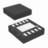
... The LMV242 is offered in fully tested die form as well 10-lead LLP package and is therefore especially suitable for small footprint PA module solutions. Typical Application VIP ® registered trademark of National Semiconductor Corporation. © 2004 National Semiconductor Corporation Features n Support of InGaP HBT, bipolar technology n Quad-band operation n Shutdown mode for power save in R ...
Page 2
... Absolute Maximum Ratings If Military/Aerospace specified devices are required, please contact the National Semiconductor Sales Office/ Distributors for availability and specifications. Supply Voltage V - GND DD ESD Tolerance (Note 2) Human Body Model Machine Model Storage Temperature Range Junction Temperature (Note 6) 2.6V Electrical Characteristics V = 2.6V. Boldface limits apply at temperature extremes (Note 4). ...
Page 3
Electrical Characteristics V = 2.6V. Boldface limits apply at temperature extremes (Note 4). (Continued) DD Symbol Parameter V Output Swing from Rail O I Output Short Circuit Current O (Note 3) e Output Referred Noise n SR Slew Rate ...
Page 4
Electrical Characteristics V = 5.0V. Boldface limits apply at temperature extremes (Note 4). (Continued) DD Symbol Parameter Error Amplifier GBW Gain-Bandwidth Product V Output Swing from Rail O I Output Short Circuit Current O (Note 3) e Output Referred ...
Page 5
Bond Pad mechanical Dimensions Signal Name Pad Number Out 1 Out 2 Comp2 RAMP TX_EN BS Comp1 GND Note: Dimensions of the bond pad coordinates are in µm Origin of the coordinates: center of the ...
Page 6
Ordering Information Package Part Number LMV242LD 10-Pin LLP LMV242LDX LMV242MDA Tested and Wafer Form LMV242MWA Block Diagram www.national.com Package Marking Transport Media 1k Units Tape and Reel 242LD 4.5k Units tape and Reel 300 Units Waffle Pack No Mark 25 ...
Page 7
Typical Performance Characteristics Supply Current vs. Supply Voltage V and Log Conformance vs. RF Input Power OUT @ 900 MHz V and Log Conformance vs. RF Input Power OUT @ 1900 MHz Unless otherwise specified and Log Conformance ...
Page 8
Typical Performance Characteristics 25˚C. (Continued) Logarithmic Slope vs. Frequency RF Input Impedance vs. Frequency @ Resistance and Reactance I vs. V COMP RAMP www.national.com Unless otherwise specified, V Logarithmic Intercept vs. Frequency 20079516 Gain and Phase vs. Frequency 20079518 20079520 ...
Page 9
Typical Performance Characteristics 25˚C. (Continued) Sourcing Current vs. Output Voltage Output Voltage vs. Sourcing Current Closed Loop P (PA) vs OUT RAMP Unless otherwise specified, V Sinking Current vs. Output Voltage 20079510 Output Voltage vs. Sinking Current 20079512 ...
Page 10
Typical Performance Characteristics 25˚C. (Continued) Closed Loop P (PA) vs. V OUT RAMP Band Closed Loop DCS-1800 MHz Band www.national.com Unless otherwise specified PCS 1900 MHz Closed Loop GSM- 900 MHz Band 20079524 Closed Loop PCS-1900 MHz Band ...
Page 11
... Application Section POWER CONTROL PRINCIPLES The LMV242 is a member of the power loop controller family of National Semiconductor, for quad-band TDMA/GSM solu- tions. The typical application diagram demonstrates a basic approach for implementing the quad-band solution around an RF Power Amplifier (PA). The LMV242 contains Logamp detector and interfaces directly with the directional coupler ...
Page 12
Application Section (Continued) We will assume initially that the output of the some low level and that the V voltage is at 1V. The V/I RAMP converter converts the V voltage to a sinking current RAMP I ...
Page 13
Application Section (Continued) Extra attenuation Z between the coupler and the RF input of the LMV242 can be achieved by 2 resistors R according to Figure 3, where LOG ( ...
Page 14
Application Section (Continued) The control loop can be configured by the following vari- ables: • Lead time TX_EN event vs. start GSM burst www.national.com • Lead time V • Ramp profile • Loop compensation FIGURE 5. Timing V vs. RF ...
Page 15
Die / Wafer Characteristics Fabrication Attributes Physical Die Identification LMV242A Die Step A Physical Attributes Wafer Diameter 200 mm Die Size (Drawn) 889 µm x 1562 µm 35.0 mils x 61.5 mils Thickness 216 µm Nominal Min Pitch 123 µm ...
Page 16
... BANNED SUBSTANCE COMPLIANCE National Semiconductor certifies that the products and packing materials meet the provisions of the Customer Products Stewardship Specification (CSP-9-111C2) and the Banned Substances and Materials of Interest Specification (CSP-9-111S2) and contain no ‘‘Banned Substances’’ as defined in CSP-9-111S2. ...