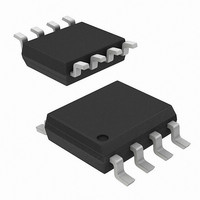
U2795B-MFPG3 Atmel, U2795B-MFPG3 Datasheet

U2795B-MFPG3
Specifications of U2795B-MFPG3
Related parts for U2795B-MFPG3
U2795B-MFPG3 Summary of contents
Page 1
... Electrostatic sensitive device. Observe precautions for handling. Description The U2795B is a 2.5-GHz mixer for WLAN and RF telecommunications equipment, e.g., DECT and PCN. The IC is manufactured using Atmel's advanced bipolar technol- ogy. A double-balanced approach was chosen to assure good isolation characteristics and a minimum of spurious products. The input and output are single-ended, and their characteristics are programmable ...
Page 2
... Pin Configuration Figure 2. Pinning Pin Description Pin Symbol Function 1 VS Supply voltage 2 RFI RF input 3 P Programming port IP3 Output symmetry 5 IFO IF output 6 GND Ground 7 LOI LO input 8 PU Power-up U2795B RFI LOI GND IFO 4654B–CELL–07/04 ...
Page 3
... S The symmetry of the load current can be matched and thus optimized for a given load impedance. Symbol stg Symbol R thJA Symbol amb U2795B with an additional capacitive component. This . P Value 125 -40 to +125 Value 175 Value 2.7 to 5.5 - Unit V V °C ° ...
Page 4
... Power-down Mode V 9.1 Supply current V 10 Power-down Voltage V 10.1 “Power ON” V 10.2 “Power DOWN” Power ON 10.3 Power-down current Power DOWN 10.4 Settling time *) Type means 100% tested 100% correlation tested Characterized on samples Design parameter U2795B system impedance Pin Symbol ...
Page 5
... Figure 3. IIP3 versus Resistor -10 0 Figure 4. OIP3 versus Resistor -10 -15 -20 -25 0 Figure 5. Gain versus Resistor R -30 dBm - IF: 900 MHz 100 IF: 900 MHz p 100 LO: 1030 MHz, level -10 dBm; RF: 130 MHz, p 100 U2795B 5 ...
Page 6
... U2795B 6 Figure 6. Supply Current I versus Resistor Figure 7. Gain versus IF Output Frequency, LO Level: -6 dBm, RF: 130 MHz, -35 dBm; Parameter: RF Input Termination 18 14 without Figure 8. IIP3 versus IF Output Frequency, LO Level: -6 dBm; RF: 130 MHz/ 130.1 MHz, -35 dBm; Parameter: RF Input Termination -10 -12 -14 with RF input matching L -16 ...
Page 7
... Figure 9. Double Sideband Noise Figure versus IF Output Frequency; LO: 1000 MHz, Level 0 dBm Input Matching Figure 10. Typical VSWR Frequency Response of the IF Output 100 Left Out T 200 400 600 800 IF (MHz) 1000 280 460 640 820 IF Frequency (MHz) U2795B = P 7 ...
Page 8
... U2795B 8 Figure 11. Typical Impedance of the Output versus R Markers (from Left to Right): R 0.5j 0.2j 0 0.2 -0.2j -0.5j Figure 12. Typical S11 Frequency Response of the IF Output, R from 100 MHz to 1000 MHz, Marker: 900 MHz 0.5j 0.2j 0 0.2 -0.2j -0.5j at Frequency /22 k /10 k /8.2 k /5.6 k ...
Page 9
... Figure 13. Typical S11 Frequency Response of the RF Input Frequency from 100 MHz to 1000 MHz, Marker: 900 MHz 0.5j 0.2j 0 0.2 -0.2j -0.5j Figure 14. Typical S11 Frequency Response of the LO Input, R from 100 MHz to 1000 MHz, Marker: 900 MHz 0.5j 0.2j 0 0.2 -0.2j - Frequency 0 -2j -j U2795B = T 5j -5j 5j -5j 9 ...
Page 10
... Application U2795B Table 1. Part List Part — — — the part-list values are used, the PU settling time is < 20 µs. Using other values, time requirements in burst-mode applications have to be considered. The values of R and R depend on the input and output condition requirements. For ...
Page 11
... Application Circuit (Evaluation Board) 4654B–CELL–07/04 U2795B 11 ...
Page 12
... Ordering Information Extended Type Number U2795B-MFP U2795B-MFPG3 Package Information Package SO8 Dimensions in mm U2795B 12 Package Remarks SO8 Tube SO8 Taped and reeled 5.00 4.85 1.4 0.25 0.4 0.10 1.27 3. technical drawings according to DIN specifications 1 4 5.2 4.8 3.7 0.2 3.8 6.15 5.85 4654B– ...
Page 13
... No licenses to patents or other intellectual property of Atmel are granted by the Company in connection with the sale of Atmel products, expressly or by implication. Atmel’s products are not authorized for use as critical components in life support devices or systems. ...


