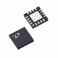
LT5521EUF Linear Technology, LT5521EUF Datasheet

LT5521EUF
Specifications of LT5521EUF
Available stocks
Related parts for LT5521EUF
LT5521EUF Summary of contents
Page 1
... The LT5521 offers exceptional LO-RF isolation, greatly reducing the need for output filtering to meet LO suppres- sion requirements. The device is designed to work over a supply voltage range from 3.15V to 5.25V. , LTC and LT are registered trademarks of Linear Technology Corporation. LO INPUT –5dBm 6.8pF LO GND ...
Page 2
... EN = 0.2V Internally Biased V = 5V, Internally Biased 3.3V, Internally Biased 5V 2.9V CONDITIONS 1700MHz O LO Requires Matching Requires Matching U W INFORMATION ORDER PART TOP VIEW NUMBER LT5521EUF + 1 12 OUT 2 11 GND GND – OUT PART MARKING UF PACKAGE 5521 4mm) PLASTIC QFN = 125 C unless otherwise noted ...
Page 3
AC ELECTRICAL CHARACTERISTICS P = –5dBm 1950MHz Test circuit shown in Figure PARAMETER Conversion Gain Conversion Gain Variation vs Temperature Input P1dB Single-Side Band Noise Figure IIP3 IIP2 (Note 6) ...
Page 4
LT5521 W U TYPICAL DC PERFOR A CE CHARACTERISTICS Supply Current vs Supply Voltage (5V Application) 100 4.7 4.8 4.9 5 TYPICAL AC PERFOR ...
Page 5
W U TYPICAL AC PERFOR A CE CHARACTERISTICS P = –5dBm 5V 2.9V unless otherwise noted. Test circuit shown in Figure 1 is tuned for 1.95GHz output frequency and ...
Page 6
LT5521 W U TYPICAL AC PERFOR A CE CHARACTERISTICS P = –5dBm 5V 2.9V unless otherwise noted. Test circuit shown in Figure 1 is tuned for 1.045GHz output frequency. ...
Page 7
W U TYPICAL AC PERFOR A CE CHARACTERISTICS P = –5dBm 5V 2.9V unless otherwise noted. Test circuit shown in Figure 1 is tuned for 1.045GHz output frequency. Noise ...
Page 8
LT5521 W U TYPICAL AC PERFOR A CE CHARACTERISTICS = –5dBm 3.3V 2.9V unless otherwise noted. Test circuit shown in Figure 1 is tuned for 1.95GHz output CC A frequency and V ...
Page 9
W BLOCK DIAGRA TEST CIRCUITS Z14 C6 Table 1. Demonstration Board Bill of Materials REF R1, R7 Z14 Z3 L1 C1, C13 C3 C12 C2, C4, C6 C11 Z1 ...
Page 10
LT5521 U U APPLICATIO S I FOR ATIO The LT5521 is a high linearity double-balanced active mixer. The chip consists of a double-balanced mixer core, a high performance LO buffer and associated bias and enable circuitry. The chip is designed ...
Page 11
U U APPLICATIO S I FOR ATIO LT5521 R1 C2 1nF + 2:1 C13 V CC 1nF – Figure 4. Low Frequency Signal Input on the IF input frequency and the ...
Page 12
LT5521 U U APPLICATIO S I FOR ATIO 3.5 IIP3 2 250MHz IF 1 1.7GHz 1.95GHz RF 0.5 –0 –1.5 –2 ...
Page 13
U U APPLICATIO S I FOR ATIO Table 6. Matching Values Using M/A-COM ETC1.6-4-2-3 Output Transformer f L1 OUT 2.4GHz 0nH 82pF 2.2GHz 1nH 82pF 2.0GHz 2.7nH 82pF 1.7GHz 4.7nH 82pF 1.3GHz 10nH 82pF 1.0GHz 10nH 3.9pF 5 ...
Page 14
LT5521 U U APPLICATIO S I FOR ATIO 0 –5 – 6.8pF –15 – 2.7pF –25 –30 –35 0 500 1000 1500 2000 2500 3000 FREQUENCY (MHz) Figure 13. LO Port Return Loss noise performance with ...
Page 15
... RECOMMENDED SOLDER PAD PITCH AND DIMENSIONS Information furnished by Linear Technology Corporation is believed to be accurate and reliable. However, no responsibility is assumed for its use. Linear Technology Corporation makes no represen- tation that the interconnection of its circuits as described herein will not infringe on existing patent rights. ...
Page 16
... Loop BW Multiband GSM/DCS/GPRS Phones, 45dB Dynamic Range, 250kHz Loop BW Multiband GSM/GPRS/EDGE Mobile Phones www.linear.com Offset Control, Shutdown, Adjustable Gain Offset Control, Shutdown, Adjustable Offset Offset Control, Adjustable Gain and Offset LT/TP 0604 1K • PRINTED IN THE USA LINEAR TECHNOLOGY CORPORATION 2004 5521f ...


