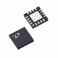
LT5519EUF Linear Technology, LT5519EUF Datasheet

LT5519EUF
Specifications of LT5519EUF
Available stocks
Related parts for LT5519EUF
LT5519EUF Summary of contents
Page 1
... The LT5519 mixer delivers +17.1dBm typical input 3rd order intercept point at 1GHz with IF input signal levels of –10dBm. The input 1dB compression point is typically +5.5dBm. The IC requires only a single 5V supply. , LTC and LT are registered trademarks of Linear Technology Corporation. 39nH CC1 ...
Page 2
... C, IF input = 140MHz at –10dBm, LO input = 1.14GHz at –5dBm, RF output measured A CONDITIONS with External Matching –10dBm/Tone 1MHz –10dBm, Single Tone Internally Biased Single-Side Band U W ORDER PART NUMBER GND 12 LT5519EUF + – GND 9 UF PART MARKING 5519 = 37 C/W JA MIN TYP MAX 1 to 400 300 to 1800 ...
Page 3
DC ELECTRICAL CHARACTERISTICS (Test Circuit Shown in Figure PARAMETER Enable (EN) Low = OFF, High = ON Turn-On Time (Note 4) Turn-Off Time (Note 4) Input Current Enable = High (ON) Enable = Low (OFF) ...
Page 4
LT5519 W U TYPICAL PERFOR A CE CHARACTERISTICS High input = 140MHz at –10dBm, LO input = 1.14GHz at –5dBm, RF output measured at 1000MHz unless ...
Page 5
W U TYPICAL PERFOR A CE CHARACTERISTICS High input = 140MHz at –10dBm, LO input = 1.14GHz at –5dBm, RF output measured at 1000MHz unless otherwise ...
Page 6
LT5519 W BLOCK DIAGRA GND + LO – LO GND TEST CIRCUIT IF IN 140MHz 0.018" 0.062" 0.018" REF DES C1 R1 EXPOSED + – PAD GND ...
Page 7
U U APPLICATIO S I FOR ATIO The LT5519 consists of a double-balanced mixer, a high performance LO buffer and bias/enable circuits. The RF and LO ports may be driven differentially; however, they are intended to be used in single-ended ...
Page 8
LT5519 U U APPLICATIO S I FOR ATIO LT5519 5pF + 5pF – Figure 4. LO Input Circuit Though the LO input is internally matched there may ...
Page 9
U U APPLICATIO S I FOR ATIO Table 4. Input Capacitor Values vs Frequency FREQUENCY CAPACITANCE (C1, C2) (MHz) (pF) 44 2200 70 820 140 220 240 68 300 39 350 27 440 18 The performance was evaluated with the ...
Page 10
LT5519 U TYPICAL APPLICATIO S 10 (10a) Top Layer Silkscreen (10b) Top Layer Metal Figure 10. Evaluation Board Layout 5519f ...
Page 11
... MOLD FLASH. MOLD FLASH, IF PRESENT, SHALL NOT EXCEED 0.15mm ON ANY SIDE 4. EXPOSED PAD SHALL BE SOLDER PLATED Information furnished by Linear Technology Corporation is believed to be accurate and reliable. However, no responsibility is assumed for its use. Linear Technology Corporation makes no represen- tation that the interconnection of its circuits as described herein will not infringe on existing patent rights. U ...
Page 12
... Modulation Bandwidth 1.8V to 5.25V Supply, 40MHz to 500MHz IF, –4dB to 57dB Linear Power Gain, 8.8MHz Baseband Bandwidth 1.8V to 5.25V Supply, 40MHz to 500MHz IF, –7dB to 56dB Linear Power Gain www.linear.com Offset Control, Adjustable Gain and Offset LT/TP 0104 1K • PRINTED IN USA LINEAR TECHNOLOGY CORPORATION 2004 5519f ...


