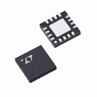
LT5512EUF Linear Technology, LT5512EUF Datasheet - Page 6

LT5512EUF
Manufacturer Part Number
LT5512EUF
Description
IC MIXER DWNCONV HI SIGN 16-QFN
Manufacturer
Linear Technology
Series
LT5512r
Datasheet
1.LT5512EUF.pdf
(12 pages)
Specifications of LT5512EUF
Rf Type
Cellular, HF, ISM, PCS, UHF, VHF, WMTS
Frequency
1kHz ~ 3GHz
Number Of Mixers
1
Gain
1.1dB
Noise Figure
14dB
Secondary Attributes
Down Converter
Current - Supply
74mA
Voltage - Supply
4.5 V ~ 5.25 V
Package / Case
16-WQFN Exposed Pad
Operating Temperature (min)
-40C
Operating Temperature (max)
85C
Operating Temperature Classification
Industrial
Lead Free Status / RoHS Status
Contains lead / RoHS non-compliant
Available stocks
Company
Part Number
Manufacturer
Quantity
Price
Part Number:
LT5512EUF
Manufacturer:
LINEAR/凌特
Quantity:
20 000
Part Number:
LT5512EUF#PBF
Manufacturer:
LINEAR/凌特
Quantity:
20 000
Company:
Part Number:
LT5512EUF#TRPBF
Manufacturer:
SP
Quantity:
5 997
Part Number:
LT5512EUF#TRPBF
Manufacturer:
LINEAR/凌特
Quantity:
20 000
PI FU CTIO S
BLOCK DIAGRA
LT5512
NC (Pins 1, 4, 8, 13, 16): Not connected internally. These
pins should be grounded on the circuit board for improved
LO to RF and LO to IF isolation.
RF
nal. These pins must be driven with a differential signal.
Each pin must be connected to a DC ground capable of
sinking 15mA (30mA total). This DC bias return can be
accomplished through the center-tap of a balun, or with
shunt inductors. An impedance transformation is required
to match the RF input to 50Ω (or 75Ω).
EN (Pin 5): Enable Pin. When the input voltage is higher
than 3V, the mixer circuits supplied through Pins 6, 7, 10,
and 11 are enabled. When the input voltage is less than
0.3V, all circuits are disabled. Typical enable pin input
current is 50μA for EN = 5V and 0μA when EN = 0V.
V
Typical current consumption is 22mA. This pin should be
externally connected to the other V
with 0.01μF and 1μF capacitors.
V
Typical current consumption is 4mA. This pin should be
6
CC1
CC2
+
U
, RF
(Pin 6): Power Supply Pin for the LO Buffer Circuits.
(Pin 7): Power Supply Pin for the Bias Circuits.
–
(Pins 2, 3): Differential Inputs for the RF Sig-
U
U
W
RF –
LO –
LO
RF
+
+
CC
15
14
2
3
pins, and decoupled
AMPLIFIER
LINEAR
HIGH-SPEED
LO BUFFER
V
CC1
6
DOUBLE-BALANCED
BACKSIDE
GROUND
17
MIXER
externally connected to the other V
with 0.01μF and 1μF capacitors.
GND (Pins 9 and 12): Ground. These pins are internally
connected to the backside ground for better isolation. They
should be connected to RF ground on the circuit board,
although they are not intended to replace the primary
grounding through the backside contact of the package.
IF
Signal. An impedance transformation may be required to
match the outputs. These pins must be connected to V
through impedance matching inductors, RF chokes or a
transformer center-tap.
LO
Oscillator Signal. They can also be driven single-ended by
connecting one to an RF ground through a DC blocking
capacitor. These pins are internally biased to 2V; thus, DC
blocking capacitors are required. An impedance transfor-
mation or matching resistor is required to match the LO
input to 50Ω (or 75Ω).
GROUND (Pin 17): (Backside Contact): Circuit Ground
Return for the Entire IC. This must be soldered to the
printed circuit board ground plane.
–
–
, IF
, LO
15mA
15mA
V
CC2
+
7
BIAS
+
(Pins 10, 11): Differential Outputs for the IF
(Pins 14, 15): Differential Inputs for the Local
12
11
10
9
5
5512 BD
GND
IF
IF –
GND
EN
+
CC
pins, and decoupled
5512fa
CC


