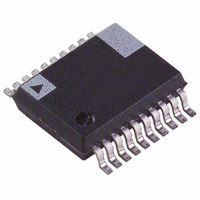
AD6459ARS Analog Devices Inc, AD6459ARS Datasheet - Page 8

AD6459ARS
Manufacturer Part Number
AD6459ARS
Description
IC RCVR IF SUBSYS GSM 3V 20-SSOP
Manufacturer
Analog Devices Inc
Datasheet
1.AD6459ARS.pdf
(12 pages)
Specifications of AD6459ARS
Rohs Status
RoHS non-compliant
Function
Receiver IF Subsystem
Frequency
500MHz
Rf Type
Cellular, GSM, IS-54, TETRA, DCS, PCS
Secondary Attributes
3V, Low Power Receiver IF Subsystem
Package / Case
20-SSOP (0.200", 5.30mm Width)
Operating Temperature (max)
85C
Operating Temperature Classification
Commercial
Operating Supply Voltage (min)
2.7V
Operating Supply Voltage (max)
5.5V
Lead Free Status / Rohs Status
Not Compliant
Available stocks
Company
Part Number
Manufacturer
Quantity
Price
Company:
Part Number:
AD6459ARS
Manufacturer:
AD
Quantity:
1 791
Part Number:
AD6459ARS
Manufacturer:
ADI/亚德诺
Quantity:
20 000
Part Number:
AD6459ARSZ
Manufacturer:
ADI/亚德诺
Quantity:
20 000
AD6459
PRODUCT OVERVIEW
The AD6459 provides most of the active circuitry required to
realize a complete low power, single-conversion superhetero-
dyne receiver, or the latter part of a double-conversion receiver,
at input frequencies up to 500 MHz, with an IF from 5 MHz to
50 MHz. The internal I/Q demodulators, and their associated
phase-locked loop, support a wide variety of modulation modes,
including n-PSK, n-QAM and GMSK. A single positive supply
voltage of 3 V is required (2.7 V minimum, 5.5 V maximum) at
a typical supply current of 8 mA at midgain. In the following
discussion, V
which will be normally assumed to be 3 V.
Figure 20 shows the main sections of the AD6459. It consists of
a variable-gain UHF mixer and a linear two-stage IF strip,
which together provide a calibrated voltage-controlled gain range
of more than 76 dB, followed by dual quadrature demodulators.
These are driven by inphase and quadrature clocks that are
generated by a Phase-Locked Loop (PLL), which is locked to a
corrected external reference. A CMOS-compatible power-down
interface completes the AD6459.
Mixer
The UHF mixer is an improved Gilbert-cell design and can
operate from low frequencies (it is internally dc-coupled) up to
an RF input of 500 MHz. The dynamic range at the input of the
POS
will be used to denote the power supply voltage,
RFLO
PRUP
VPS1
VPS2
RFHI
18
20
5
6
3
LOIP
4
CIRCUIT
BIAS
MXOM
MXOP
10
9
Figure 20. Functional Block Diagram
COM1
BANDPASS
2
FILTER
LC
COM2
AGC VOLTAGE
7
11
12
IFIP
IFIM
–8–
+
–
mixer is determined, at the upper end, by the maximum input
signal level of 90 mV (–11 dBm in 50
RFLO) up to which the mixer remains essentially linear, and at
the lower end, by the noise level. It is customary to define the
linearity of a mixer in terms of its 1 dB gain-compression point
and third-order intercept, which for the AD6459 are –11 dBm
and 0 dBm, respectively, in a 50
The mixer’s RF input port is differential; that is, pin RFLO is
functionally identical to RFHI, and these nodes are internally
biased. The RF port can be modeled as a parallel RC circuit as
shown in Figure 19.
The local oscillator (LO) input is internally biased at V
and must be ac coupled. The LO interface includes a preampli-
fier that minimizes the drive requirements, thus simplifying the
oscillator design and reducing LO leakage from the RF port.
The LO requires a single-sided drive of 50 mV, or –16 dBm
in a 50
can be improved by increasing the LO level.
AD6459
Figure 19. Mixer Port Modeled as a Parallel RC Network
system. For operation above 300 MHz, noise figure
COMPENSATION
PLL
GAIN TO
0
50
RFLO
RFHI
4.7k
4.7k
4.7k
4.7k
C
system.
16
17
19
15
14
13
SH
1
8
IRXP
IRXN
FREF
FLTR
QRXP
QRXN
GAIN
GREF
R
between RFHI and
SH
P
–0.8 V
REV. 0


