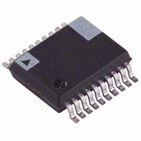
AD607ARS Analog Devices Inc, AD607ARS Datasheet - Page 16

AD607ARS
Manufacturer Part Number
AD607ARS
Description
IC LIN RCVR IF SUBSYS LP 20-SSOP
Manufacturer
Analog Devices Inc
Datasheet
1.AD607-EBZ.pdf
(24 pages)
Specifications of AD607ARS
Rohs Status
RoHS non-compliant
Function
Receiver IF Subsystem
Frequency
500MHz
Rf Type
Cellular, GSM, CDMA, TDMA, TETRA
Secondary Attributes
-8dBm Input Third Order Intercept
Package / Case
20-SSOP (0.200", 5.30mm Width)
Operating Supply Voltage
3V
Operating Temperature (min)
-40C
Operating Temperature (max)
85C
Operating Temperature Classification
Industrial
Lead Free Status / Rohs Status
Not Compliant
Available stocks
Company
Part Number
Manufacturer
Quantity
Price
Company:
Part Number:
AD607ARS
Manufacturer:
AD
Quantity:
5 510
Company:
Part Number:
AD607ARS
Manufacturer:
NEC
Quantity:
5 510
Part Number:
AD607ARS
Manufacturer:
ADI/亚德诺
Quantity:
20 000
Company:
Part Number:
AD607ARSZ
Manufacturer:
ADI
Quantity:
730
Part Number:
AD607ARSZ
Manufacturer:
ADI/亚德诺
Quantity:
20 000
AD607
The IF’s small-signal bandwidth is approximately 45 MHz from
IFHI and IFLO through IFOP. The peak output at IFOP is
± 560 mV at V
2.92 V. This allows some headroom at the demodulator inputs
(Pin DMIP), which accept a maximum input of ± 150 mV for
IFs > 3 MHz and ± 75 mV for IFs ≤ 3 MHz (at IFs ≤ 3 MHz,
the drive to the demodulators must be reduced to avoid saturat-
ing the output amplifiers with higher order mixing products that
are no longer removed by the on-board low pass filters).
Since there is no band-limiting in the IF strip, the output-
referred noise can be quite high; in a typical application and
at a gain of 75 dB, it is about 100 mV rms, making post-IF filtering
desirable. IFOP may be also used as an IF output for driving
an A/D converter, external demodulator, or external AGC
detector. Figure 17 shows methods of matching the optional
second IF filter.
Gain Scaling and RSSI
The AD607’s overall gain, expressed in decibels, is linear-in-dB
with respect to the AGC voltage V
all sections is maximum when V
sively up to V
V
features temperature compensation of the gain scaling. The gain
control scaling is proportional to the reference voltage applied to
the Pin GREF. When this pin is tied to the midpoint of the
supply (VMID), the scale is nominally 20 mV/dB (50 dB/V) for
V
(mixer plus IF) corresponds to a control voltage of 0.4 V ≤
V
the insertion losses of the IF filters used. More generally, the gain
scaling using these connections is V
becomes 33.3 mV/dB (30 dB/V) using a 5 V supply, with a
proportional change in the AGC range, to 0.33 V ≤ V
a. Biasing DMIP from Power Supply (Assumes BPF
AC-Coupled Internally)
b. Biasing DMIP from VMID (Assumes BPF AC-Coupled
Internally)
P
P
G
Figure 17. Input and Output Matching of the Optional
Second IF Filter
– 0.8 V). The gain of all stages changes in parallel. The AD607
= 3 V. Under these conditions, the lower 80 dB of gain range
≤ 2.0 V. The final centering of this 1.6 V range depends on
G
P
= 2.2 V (for V
= 3 V and ± 400 mV at the minimum V
AD607
AD607
DMIP
IFOP
DMIP
VMID
IFOP
P
R
T
= 3 V; in general, up to a limit
R
G
T
is zero, and reduces progres-
G
C
P
BYPASS
BPF
at Pin GAIN. The gain of
/150 (volts per dB), so scale
BPF
R
VPOS
T
2R
2R
T
T
G
≤ 3 V.
P
of
–16–
Table II lists gain control voltages and scale factors for power
supply voltages from 2.92 V to 5.5 V
Alternatively, Pin GREF can be tied to an external voltage
reference (V
AD1580 (1.21 V) voltage reference, to provide supply-
independent gain scaling of V
the Analog Devices’ AD7013 and AD7015 baseband converters,
the external reference may also be provided by the reference
output of the baseband converter (Figure 18). For example, the
AD7015 baseband converter provides a V
connected to GREF, the gain scaling is 16.4 mV/dB (60 dB/V).
An auxiliary DAC in the AD7015 can be used to generate the
MGC voltage. Since it uses the same reference voltage, the
numerical input to this DAC provides an accurate RSSI value
in digital form, no longer requiring the reference voltage to have
high absolute accuracy.
Figure 18. Interfacing the AD607 to the AD7013 or AD7015
Baseband Converters
I/Q Demodulators
Both demodulators (I and Q) receive their inputs at Pin DMIP.
Internally, this single-sided input is actually differential; the
noninverting input is referenced to Pin VMID. Each demodula-
tor comprises a full-wave synchronous detector followed by a
2 MHz, two-pole low-pass filter, producing single-sided outputs
at pins IOUT and QOUT. Using the I and Q demodulators for
IFs above 12 MHz is precluded by the 400 kHz to 12 MHz
response of the PLL used in the demodulator section. Pin DMIP
requires an external bias source at V
suggested methods.
Outputs IOUT and QOUT are centered at V
up to ±1.23 V even at the low supply voltage of 2.92 V. They can
therefore directly drive the RX ADCs in the AD7015 baseband
converter, which require an amplitude of 1.23 V to fully load
them when driven by a single-sided signal. The conversion gain of
the I and Q demodulators is 18 dB (X8), requiring a maxi-
mum input amplitude at DMIP of ± 150 mV for IFs > 3 MHz.
AD607
R
) from, for example, an AD1582 (2.5 V) or
QOUT
GREF
GAIN
VMID
IOUT
R
R
10nF
R
/75 (volts per dB). When using
C
1nF
C
P
/2; Figure 19 shows
R
IADC
QADC
IADC
QADC
REFOUT
BYPASS
AUX DAC
of 1.23 V; when
AD7013 OR
P
AD7015
/2 and can swing
(AD7015)
(AD7013)
REV. C


