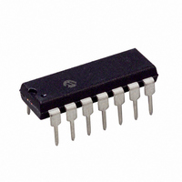
MCP2030-I/P Microchip Technology, MCP2030-I/P Datasheet - Page 46

MCP2030-I/P
Manufacturer Part Number
MCP2030-I/P
Description
IC KEYLESS ENTRY AFE 14DIP
Manufacturer
Microchip Technology
Datasheet
1.MCP2030-ISL.pdf
(66 pages)
Specifications of MCP2030-I/P
Rf Type
ISM
Frequency
125kHz
Features
10kbps
Package / Case
14-DIP (0.300", 7.62mm)
Ic Function
Analog Front End Device IC
Supply Voltage Range
2V To 3.6V
Operating Temperature Range
-40°C To +85°C
Digital Ic Case Style
DIP
No. Of Pins
14
Supply Voltage
2V
Leaded Process Compatible
Yes
Rohs Compliant
Yes
Lead Free Status / RoHS Status
Lead free / RoHS Compliant
Available stocks
Company
Part Number
Manufacturer
Quantity
Price
Company:
Part Number:
MCP2030-I/P
Manufacturer:
MICROCHIP
Quantity:
12 000
MCP2030
5.30.3.1
The RSSI output is an analog current. It needs an
external Analog-to-Digital (ADC) data conversion
device for digitized output. The ADC data conversion
can be accomplished by using a stand-alone external
ADC device, an external MCU that has internal ADC
features, or an external MCU that has no ADC features
but instead uses firmware. The RSSIFET is used to
discharge any external charge on the LFDATA pin in
the RSSI Output mode. The MOSFET can be turned on
or off with bit RSSIFET<8> of Configuration Register 2
(Register 5-3). When it is turned on, the internal
MOSFET provides a discharge path for the external
capacitor that is connected at the LFDATA pin. This
MOSFET option is valid only if RSSI output is selected
and not controllable by users for demodulated or carrier
clock output options.
See separate application notes for various external ADC
implementation methods for this device.
See Figure 5-8 for RSSI output path.
FIGURE 5-9:
DS21981A-page 46
LFDATA/CCLK/SDIO
ANALOG-TO-DIGITAL DATA
CONVERSION OF RSSI SIGNAL
SCLK/ALERT
Power-Up Sequence.
CS
LFDATA
(output)
(open collector
ALERT
output)
5.31
5.31.1
The SPI communication is used to read from or write to
the Configuration registers and to send command-only
messages.
communication: CS, SCLK/ALERT, and LFDATA/RSSI/
CCLK/SDIO. Figure 5-9, Figure 5-10 and Figure 5-11
show examples of the SPI communication sequences.
When these pins are connected to the external MCU
I/O pins, the following are needed:
CS
• Pin is permanently an input with an internal pull-up.
SCLK/ALERT
• Pin is an open collector output when CS is high.
LFDATA/CCLK/SDIO
• Pin is a digital output (LFDATA) so long as CS is
An internal pull-up resistor exists to ensure no
spurious SPI communication between powering
and the MCU configuring its pins. This pin
becomes the SPI clock input when CS is low.
high. During SPI communication, the pin is the
SPI data input (SDI) unless performing a register
Read, where it will be the SPI data output (SDO).
C
onfiguration Registers
SPI COMMUNICATION
Three
pins
© 2005 Microchip Technology Inc.
are
used
for
SPI


