RF2713PCK-M RFMD, RF2713PCK-M Datasheet - Page 4
RF2713PCK-M
Manufacturer Part Number
RF2713PCK-M
Description
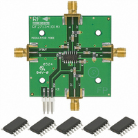
KIT EVAL FOR RF2713 MODULATOR
Manufacturer
RFMD
Type
Modulator, Demodulatorr
Datasheet
1.RF2713PCK-D.pdf
(16 pages)
Specifications of RF2713PCK-M
Frequency
0Hz ~ 250MHz
For Use With/related Products
RF2713 MODULATOR
Lead Free Status / RoHS Status
Lead free / RoHS Compliant
Other names
689-1042
Available stocks
Company
Part Number
Manufacturer
Quantity
Price
Company:

Part Number:
RF2713PCK-M
Manufacturer:
RFMD
Quantity:
5 000


RF2713
4 of 16
Pin
10
11
12
1
2
3
4
5
6
7
8
9
Q INPUT A
Q INPUT B
I INPUT A
I INPUT B
Function
Q IF OUT
BG OUT
I IF OUT
Q OUT
I OUT
GND
GND
GND
Description (Demodulator Configuration)
When the RF2713 is configured as a Quadrature Demodulator, both mixers
are driven by the IF. Whether driving the mixers single-endedly (as shown in
the application schematic) or differentially, the A Inputs (pins 1 and 3)
should be connected to each other. Likewise, both B Inputs (pins 2 and 4)
should be connected to each other. This ensures that the IF will reach each
mixer with the same amplitude and phase, yielding the best I and Q output
amplitude and quadrature balance. Note that connecting the inputs in par-
allel changes the input impedance (see the Gilbert Cell mixer equivalent
circuit). The single-ended input impedance (as shown in the application cir-
cuit) becomes 630Ω, but in the balanced configuration, the input imped-
ance would remain 1260Ω.
The mixers are Gilbert Cell designs with balanced inputs. The equivalent
schematic for one of the mixers is shown on the following page. The input
impedance of each pin is determined by the 1260Ω resistor to V
allel with a transistor base. Note from the schematic that all four input pins
have an internally set DC bias. For this reason, all four inputs (pins 1
through 4) should be DC blocked. The capacitance values of the blocking
capacitors is determined by the IF frequency. When driving single-endedly,
both the series (pins 1 and 3) and shunt (pins 2 and 4) blocking capacitors
should be low impedances, relative to the 630Ω input impedance.
Same as pin 1, except complementary input.
Same as pin 1, except Q Buffer Amplifier.
Same as pin 3, except complementary input.
Band Gap voltage reference output. This voltage output is held constant
over variations in supply voltage and operating temperature and may be
used as a reference for other external circuitry. This pin should not be
loaded such that the sourced current exceeds 1mA. This pin should be
bypassed with a large (0.1μF) capacitor.
This pin is not used in the Demodulator Configuration, but must be con-
nected to V
Same as pin 6, except Q mixer.
Q Mixer’s Baseband Output. This pin is NOT internally DC blocked and has
DC present due to internal biasing. This is an emitter-follower type output
with an internal 2kΩ pull-down resistor. Even though the AC output imped-
ance is ~50Ω, this pin is intended to drive only high impedance loads such
as an opamp or an ADC. The output transistor is NOT biased such that it
can drive a large signal into a 50Ω load. DC coupling of this output is per-
mitted provided that the DC impedance to ground, which appears in paral-
lel with the internal pull-down resistor, is significantly greater than 2kΩ.
Same as pin 8, except Q Mixer’s Baseband Output.
Ground connection. Keep traces physically short and connect immediately
to ground plane for best performance.
Same as pin 10.
Same as pin 10.
7628 Thorndike Road, Greensboro, NC 27409-9421 · For sales or technical
support, contact RFMD at (+1) 336-678-5570 or sales-support@rfmd.com.
CC
in order to properly bias the I mixer.
CC
in par-
INPUT A
Interface Schematic
See pin 1.
See pin 1.
See pin 1.
Same as pin 6.
Same as pin 8.
V
CC
1260 Ω
V
CC
2 kΩ
Rev A6 DS080403
I/Q OUT
IF OUT
V
CC
1260 Ω
INPUT B
Related parts for RF2713PCK-M
Image
Part Number
Description
Manufacturer
Datasheet
Request
R

Part Number:
Description:
IC AMP HBT GAAS CATV 8-SOIC
Manufacturer:
RFMD
Datasheet:

Part Number:
Description:
IC AMP MMIC GAAS 12GHZ 4-MICROX
Manufacturer:
RFMD
Datasheet:

Part Number:
Description:
IC AMP 3V LOW-NOISE SOT23-6
Manufacturer:
RFMD
Datasheet:

Part Number:
Description:
KIT EVAL FOR NBB-310
Manufacturer:
RFMD
Datasheet:
Part Number:
Description:
IC AMPLIFIER MMIC LNA 8-QFN
Manufacturer:
RFMD
Datasheet:
Part Number:
Description:
IC AMP MMIC GAAS 4GHZ 4-MICROX
Manufacturer:
RFMD
Datasheet:
Part Number:
Description:
IC SWITCH 10W PHEMT SPDT 12QFN
Manufacturer:
RFMD
Datasheet:
Part Number:
Description:
IC QUADRATURE MODULATOR 16-SOIC
Manufacturer:
RFMD
Datasheet:
Part Number:
Description:
100MHZ TO 4000MHZ, GAAS PHEMT MMIC LOW NOISE AMPLIFIERS
Manufacturer:
RFMD
Part Number:
Description:
KIT EVAL FOR RF2336
Manufacturer:
RFMD
Datasheet:


Part Number:
Description:
IC AMP WLAN/LNA DVR 3V SOT23-5
Manufacturer:
RFMD
Datasheet:

Part Number:
Description:
IC AMP HBT GAAS LNA BYPASS 8-QFN
Manufacturer:
RFMD
Datasheet:

Part Number:
Description:
IC AMP MMIC GAAS 10GHZ 4-MICROX
Manufacturer:
RFMD
Datasheet: