AA003257-G Navman Wireless, AA003257-G Datasheet - Page 5
AA003257-G
Manufacturer Part Number
AA003257-G
Description
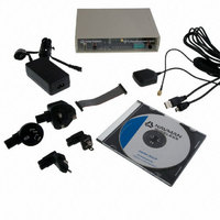
DEV KIT FOR JUPITER 32XLP
Manufacturer
Navman Wireless
Type
Receiver, GPSr
Specifications of AA003257-G
Frequency
1575.42MHz
For Use With/related Products
Jupiter 32 XLP
Lead Free Status / RoHS Status
Lead free / RoHS Compliant
Other names
943-1001
Available stocks
Company
Part Number
Manufacturer
Quantity
Price
Company:

Part Number:
AA003257-G
Manufacturer:
Navman Wireless
Quantity:
135


2.1.1 Compatibility
2.2 Receiver architecture
The functional architecture of the Jupiter 32 xLP receiver is shown in Figure 2-1.
2.3 Major components of the Jupiter 32 xLP
Bandpass SAW filter (1.575 GHz): This filters the GPS signal and removes unwanted signals
caused by external influences that would corrupt the operation of the receiver. The filtered signal
is fed to the RF input of GSC3f chipset for further processing. The filter has a bandwidth of
2 MHz.
Battery power: The back-up battery supply feeds the VDD_RTC regulator through the OR-ing
circuit, and provides the power to the battery-backed SRAM and the RTC section of the GSC3f.
Bias T: This provides the voltage to an external active antenna.
Brown out detector: The precision voltage detector chip senses the input voltage and resets
the module in case of any drop in the voltage. This detector chip also serves the function of
power-on-reset.
GSC3f chip: This single chip GPS device includes an integrated Baseband, RF section and
integrated Flash which stores software, long term and user configuration data.
LNA (Low Noise Amplifier): This amplifies the GPS signal and provides enough gain for the
receiver to use a passive antenna. A very low noise design is utilised to provide maximum
sensitivity.
LNA switch: The LNA switch controls the LNA during low power modes.
Main power: The primary supply voltage range is 3.0 to 3.6 V.
OR-ing circuit: This circuit distributes the RTC/SRAM voltage from either the main voltage
supply or the back-up voltage input in order for the RTC/SRAM elements to work in low power
and continuous modes. However a back-up voltage must be connected if the device is to be shut
down and required to perform Hot and Warm starts.
Regulator: This dual low-noise regulator provides two outputs of 2.85 V power to the RF section
and the digital IO section of the GSC3f chip.
LA000267D © 2008 Navman Wireless OEM. All rights reserved. Proprietary information and specifications subject to change without notice.
The Jupiter 32 xLP is 100% backward compatible to Jupiter 32 and identical in function and
electrical compatibility to the Jupiter 30 but has advanced miniature packaging, with a smaller
form factor (17.0 x 15.0 mm). It features the ability to save user configurations to flash memory
and uses the latest SiRFInstantFix technology for improved performance.
bias T
active or passive antenna
LNA
switch
LNA
V_ANT
input
Figure 2-1: Jupiter 32 xLP architecture
TCXO
SAW
filter
LNA_EN
XTAL_IN
RTC crystal
RFIN
combined RF/baseband device/4 Mb Flash device
VCC_RF
controls/
GPIO
regulator
VDD_BB
UART
ports
GSC3f LPx
2.9 V threshold
brown-out
3 - 3.6 V in
detector
SRESET
power
main
VDD_RTC
VDD_RTC
1.9 - 3.6 V
regulator
battery
OR-ing
power
circuit
Related parts for AA003257-G
Image
Part Number
Description
Manufacturer
Datasheet
Request
R

Part Number:
Description:
ANTENNA GPS ACTIVE 5M CABLE
Manufacturer:
Navman Wireless
Datasheet:

Part Number:
Description:
DEV KIT FOR JUPITER 30XLP
Manufacturer:
Navman Wireless
Datasheet:

Part Number:
Description:
DEV KIT FOR JUPITER 3 AND J3-30
Manufacturer:
Navman Wireless
Datasheet:

Part Number:
Description:
TERMINAL MDT-860 MOBILE DATA
Manufacturer:
Navman Wireless
Datasheet:


Part Number:
Description:
MODULE GPS RECEIVER JUPITER 3
Manufacturer:
Navman Wireless
Datasheet:

Part Number:
Description:
MODULE GPS JUPITER 30XLP 20CH
Manufacturer:
Navman Wireless
Datasheet:

Part Number:
Description:
MODULE GPS JUPITER 32XLP 20CH
Manufacturer:
Navman Wireless
Datasheet:

Part Number:
Description:
MODULE GPS RECEIVER JUPITER 3-30
Manufacturer:
Navman Wireless
Datasheet:

Part Number:
Description:
MODULE JUPITER 31 GPS W/R/A OSX
Manufacturer:
Navman Wireless
Datasheet:

Part Number:
Description:
MODULE GPS RECEIVER JUPITER 2
Manufacturer:
Navman Wireless
Datasheet:

Part Number:
Description:
DEV KIT FOR MDT860
Manufacturer:
Navman Wireless
Datasheet:

Part Number:
Description:
EVAL KIT GPS JUPITER 2
Manufacturer:
Navman Wireless
Datasheet: