1321XNSK-BDM Freescale Semiconductor, 1321XNSK-BDM Datasheet - Page 61
1321XNSK-BDM
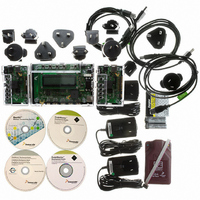
Manufacturer Part Number
1321XNSK-BDM
Description
KIT STARTER NETWORK 1321X W/USB
Manufacturer
Freescale Semiconductor
Type
Range Test Demor
Specifications of 1321XNSK-BDM
Frequency
2.4GHz
Wireless Frequency
2.4 GHz
Interface Type
SPI
Modulation
DSSS OQPSK
Security
128 bit AES
Operating Voltage
2 VDC to 3.4 VDC
Output Power
2 dBm
Antenna
F-Antenna
Operating Temperature Range
- 40 C to + 85 C
For Use With/related Products
MC1321x
Lead Free Status / RoHS Status
Lead free / RoHS Compliant


6.4.3
Table 20
Freescale Semiconductor
No.
10
1
2
3
4
5
6
7
8
9
(CPOL = 1)
(CPOL = 0)
(OUTPUT)
(OUTPUT)
(OUTPUT)
(OUTPUT)
(INPUT)
describes the timing requirements for the SPI system.
MISO
MOSI
Operating frequency
SCK period
Enable lead time
Enable lag time
Clock (SCK) high or low time
Data setup time (inputs)
Data hold time (inputs)
Data valid (after SCK edge)
Data hold time (outputs)
Rise time
Fall time
SCK
SCK
SS
System SPI Timing
Master
Master
Master
Master
Master
Master
Master
Master
Master
Input
Output
Input
Output
1
5
Function
2
MSB IN
MSB OUT
6
2
Figure 33. SPI Master Timing (CPHA = 0)
4
MC13211/212/213 Technical Data, Rev. 1.8
2
1
Table 20. SPI Timing
4
BIT 6 . . . 1
BIT 6 . . . 1
7
Symbol
t
WSCK
t
t
t
Lead
t
t
SCK
t
t
f
Lag
t
t
HO
RO
t
SU
FO
t
op
HI
RI
FI
v
f
Bus
LSB IN
62.5
Min
LSB OUT
1/2
1/2
15
—
—
—
—
—
/2048
2
0
0
10
9
f
Bus
1024 t
t
t
/2 = 8 MHz
cyc
cyc
2048
Max
8
—
—
—
—
25
—
25
25
– 25
– 25
cyc
3
Unit
t
t
t
SCK
SCK
Hz
ns
ns
ns
ns
ns
ns
ns
ns
ns
cyc
61
Related parts for 1321XNSK-BDM
Image
Part Number
Description
Manufacturer
Datasheet
Request
R

Part Number:
Description:
KIT STARTER NETWORK FOR 1321X
Manufacturer:
Freescale Semiconductor
Datasheet:

Part Number:
Description:
Manufacturer:
Freescale Semiconductor, Inc
Datasheet:
Part Number:
Description:
Manufacturer:
Freescale Semiconductor, Inc
Datasheet:
Part Number:
Description:
Manufacturer:
Freescale Semiconductor, Inc
Datasheet:
Part Number:
Description:
Manufacturer:
Freescale Semiconductor, Inc
Datasheet:
Part Number:
Description:
Manufacturer:
Freescale Semiconductor, Inc
Datasheet:
Part Number:
Description:
Manufacturer:
Freescale Semiconductor, Inc
Datasheet:
Part Number:
Description:
Manufacturer:
Freescale Semiconductor, Inc
Datasheet:
Part Number:
Description:
Manufacturer:
Freescale Semiconductor, Inc
Datasheet:
Part Number:
Description:
Manufacturer:
Freescale Semiconductor, Inc
Datasheet:
Part Number:
Description:
Manufacturer:
Freescale Semiconductor, Inc
Datasheet:
Part Number:
Description:
Manufacturer:
Freescale Semiconductor, Inc
Datasheet:
Part Number:
Description:
Manufacturer:
Freescale Semiconductor, Inc
Datasheet:
Part Number:
Description:
Manufacturer:
Freescale Semiconductor, Inc
Datasheet:
Part Number:
Description:
Manufacturer:
Freescale Semiconductor, Inc
Datasheet: