SM1211E915TOPIC Semtech, SM1211E915TOPIC Datasheet - Page 38
SM1211E915TOPIC
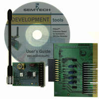
Manufacturer Part Number
SM1211E915TOPIC
Description
KIT PICTAIL EXT FOR SX1211
Manufacturer
Semtech
Type
Transceiver, UHFr
Specifications of SM1211E915TOPIC
Frequency
915MHz
For Use With/related Products
SX1211
Lead Free Status / RoHS Status
Lead free / RoHS Compliant


To read bytes from the FIFO the timing diagram below should be carefully followed by the uC.
Note that it is compulsory to toggle NSS_DATA back high between each byte read.
In Buffered and Packet modes of operation, both data to be transmitted and that has been received are stored in a
configurable FIFO (First In First Out) device. It is accessed via the SPI Data interface and provides several
interrupts for transfer management.
The FIFO is 1 byte (8 bits) wide hence it only performs byte (parallel) operations, whereas the demodulator
functions serially. A shift register is therefore employed to interface the two devices. In transmit mode it takes bytes
from the FIFO and outputs them serially (MSB first) at the programmed bit rate to the modulator. Similarly, in Rx the
shift register gets bit by bit data from the demodulator and writes them byte by byte to the FIFO. This is illustrated in
figure below.
The FIFO width is programmable, to 16, 32, 48 or 64 bytes via MCParam_Fifo_size
Rev 7 – Sept 2
ADVANCED COMMUNICATIONS & SENSING
Read Byte (after/during Rx)
NSS_DATA (In)
SCK (In)
MOSI (In)
MISO (Out)
5.2.2. FIFO
nd
, 2008
HZ
(input)
5.2.2.1. Overview and Shift Register (SR)
5.2.2.2. Size Selection
D1(7)
1
x
D1(6) D1(5)
x
2
x
3
Data Tx/Rx
1
Figure 30: Read Bytes Sequence (ex: 2 bytes)
D1(4) D1(3)
st
4
x
byte read
Figure 31: FIFO and Shift Register (SR)
5
x
1
D1(2) D1(1)
6
x
MSB
7
x
Page 38 of 92
D1(0)
8
x
SR (8bits)
x
(input)
byte1
byte0
HZ
8
D2(7) D2(6)
1
x
2
x
LSB
D2(5)
3
x
FIFO
2
D2(4)
nd
4
x
byte read
D2(3)
5
x
D2(2)
6
x
D2(1)
7
x
D2(0)
8
x
www.semtech.com
SX1211
HZ
(input)
Related parts for SM1211E915TOPIC
Image
Part Number
Description
Manufacturer
Datasheet
Request
R

Part Number:
Description:
Ultra Low Power Integrated Uhf Transceiver Module
Manufacturer:
Semtech Corporation
Datasheet:

Part Number:
Description:
EVALUATION BOARD
Manufacturer:
Semtech
Datasheet:
Part Number:
Description:
EVALUATION BOARD
Manufacturer:
Semtech
Datasheet:
Part Number:
Description:
VOLTAGE SUPPRESSOR, TRANSIENT SEMTECH
Manufacturer:
Semtech
Datasheet:
Part Number:
Description:
HIGH VOLTAGE CAPACITORS MONOLITHIC CERAMIC TYPE
Manufacturer:
Semtech Corporation
Datasheet:
Part Number:
Description:
EZ1084CM5.0 AMP POSITIVE VOLTAGE REGULATOR
Manufacturer:
Semtech Corporation
Datasheet:
Part Number:
Description:
3.0 AMP LOW DROPOUT POSITIVE VOLTAGE REGULATORS
Manufacturer:
Semtech Corporation
Datasheet:
Part Number:
Description:
Manufacturer:
Semtech Corporation
Datasheet:
Part Number:
Description:
RailClamp Low Capacitance TVS Diode Array
Manufacturer:
Semtech Corporation
Datasheet:
Part Number:
Description:
Manufacturer:
Semtech Corporation
Datasheet:
Part Number:
Description:
Manufacturer:
Semtech Corporation
Datasheet:
Part Number:
Description:
Manufacturer:
Semtech Corporation
Datasheet: