RF2637PCK-410 RFMD, RF2637PCK-410 Datasheet - Page 2
RF2637PCK-410
Manufacturer Part Number
RF2637PCK-410
Description
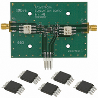
KIT EVAL FOR RF2637
Manufacturer
RFMD
Type
Amplifierr
Datasheet
1.RF2637TR7.pdf
(10 pages)
Specifications of RF2637PCK-410
Frequency
12MHz ~ 385MHz
For Use With/related Products
RF2637
Lead Free Status / RoHS Status
Lead free / RoHS Compliant
Other names
689-1058
Available stocks
Company
Part Number
Manufacturer
Quantity
Price
Company:

Part Number:
RF2637PCK-410
Manufacturer:
RFMD
Quantity:
5 000


RF2637
2 of 10
Absolute Maximum Ratings
Supply Voltage
Control Voltage
Input RF Power
Operating Ambient Temperature
Storage Temperature
Overall
Frequency Range
Maximum Gain
Minimum Gain
Maximum Gain
Minimum Gain
Gain Slope
Gain Control Voltage Range
Gain Control Input Impedance
Noise Figure
Input IP
Stability (Max VSWR)
IF Input
Input Impedance
Power Supply
Voltage
Current Consumption
Thermal
Thermal Resistance
Maximum Junction Temperature
Note 1: Measured between a gain control voltage of 1.0V to 1.5V.
3
Parameter
Parameter
7628 Thorndike Road, Greensboro, NC 27409-9421 · For sales or technical
support, contact RFMD at (+1) 336-678-5570 or sales-support@rfmd.com.
Min.
+40
+35
10:1
-65
-68
-46
7
6
-0.5 to +5.0
-0.5 to +5.0
-40 to +150
-40 to +85
Value
Specification
+10
12 to 385
2.7 to 3.4
0 to 2.5
Typ.
11.5
+45
150
+51
-55
-58
-40
57
30
10
90
-2
5
1
Max.
Unit
dBm
V
V
+65
+55
-40
-48
7.2
15
15
°C
°C
DC
DC
Exceeding any one or a combination of the Absolute Maximum Rating conditions may
cause permanent damage to the device. Extended application of Absolute Maximum
Rating conditions to the device may reduce device reliability. Specified typical perfor-
mance or functional operation of the device under Absolute Maximum Rating condi-
tions is not implied.
RoHS status based on EUDirective2002/95/EC (at time of this document revision).
The information in this publication is believed to be accurate and reliable. However, no
responsibility is assumed by RF Micro Devices, Inc. ("RFMD") for its use, nor for any
infringement of patents, or other rights of third parties, resulting from its use. No
license is granted by implication or otherwise under any patent or patent rights of
RFMD. RFMD reserves the right to change component circuitry, recommended appli-
cation circuitry and specifications at any time without prior notice.
°C/W
Unit
dB/V
dBm
dBm
MHz
V
kΩ
kΩ
mA
mA
dB
dB
dB
dB
dB
°C
DC
V
Caution! ESD sensitive device.
T=25°C, 85MHz, V
Z
Resistor, 500Ω External Output Terminating
Resistor (Effective Z
Z
V
V
V
V
Note 1
Source impedance of 4.7kΩ
At maximum gain and 85MHz
At +40dB gain, referenced to 500Ω
At minimum gain, referenced to 500Ω
Spurious<-70dBm
CDMA, differential
Minimum gain, V
Maximum gain, V
Theta J-Ref 85°C
Ref 85°C
L
L
GC
GC
GC
GC
=500Ω, 500Ω External Input Terminating
=250Ω) (See Application Example)
=2.5V, 85MHz
=0.1V, 85MHz
=2.5V, 385MHz
=0.1V, 385MHz
CC
Condition
CC
CC
=3.0V
S
=3.0V
=333Ω, Effective
=3.0V, Z
Rev A6 DS080403
S
=500Ω,
Related parts for RF2637PCK-410
Image
Part Number
Description
Manufacturer
Datasheet
Request
R

Part Number:
Description:
IC AMP HBT GAAS CATV 8-SOIC
Manufacturer:
RFMD
Datasheet:

Part Number:
Description:
IC AMP MMIC GAAS 12GHZ 4-MICROX
Manufacturer:
RFMD
Datasheet:

Part Number:
Description:
IC AMP 3V LOW-NOISE SOT23-6
Manufacturer:
RFMD
Datasheet:

Part Number:
Description:
KIT EVAL FOR NBB-310
Manufacturer:
RFMD
Datasheet:
Part Number:
Description:
IC AMPLIFIER MMIC LNA 8-QFN
Manufacturer:
RFMD
Datasheet:
Part Number:
Description:
IC AMP MMIC GAAS 4GHZ 4-MICROX
Manufacturer:
RFMD
Datasheet:
Part Number:
Description:
IC SWITCH 10W PHEMT SPDT 12QFN
Manufacturer:
RFMD
Datasheet:
Part Number:
Description:
IC QUADRATURE MODULATOR 16-SOIC
Manufacturer:
RFMD
Datasheet:
Part Number:
Description:
100MHZ TO 4000MHZ, GAAS PHEMT MMIC LOW NOISE AMPLIFIERS
Manufacturer:
RFMD
Part Number:
Description:
KIT EVAL FOR RF2336
Manufacturer:
RFMD
Datasheet:


Part Number:
Description:
IC AMP WLAN/LNA DVR 3V SOT23-5
Manufacturer:
RFMD
Datasheet:

Part Number:
Description:
IC AMP HBT GAAS LNA BYPASS 8-QFN
Manufacturer:
RFMD
Datasheet:

Part Number:
Description:
IC AMP MMIC GAAS 10GHZ 4-MICROX
Manufacturer:
RFMD
Datasheet: