RF2483PCK-410 RFMD, RF2483PCK-410 Datasheet - Page 11
RF2483PCK-410
Manufacturer Part Number
RF2483PCK-410
Description
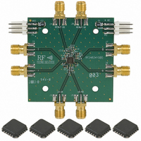
KIT EVAL FOR RF2483
Manufacturer
RFMD
Type
Modulatorr
Datasheet
1.RF2483PCK-410.pdf
(28 pages)
Specifications of RF2483PCK-410
Frequency
700MHz ~ 2.4GHz
For Use With/related Products
RF2483
Lead Free Status / RoHS Status
Lead free / RoHS Compliant
Other names
689-1040
Available stocks
Company
Part Number
Manufacturer
Quantity
Price
Company:

Part Number:
RF2483PCK-410
Manufacturer:
RFMD
Quantity:
5 000


Rev A9 DS080403
Flag
Pin
Die
19
20
RF OUT HB
Function
GND3
GND4
Description
RF high band output. Open collector output.
The output should be biased at VCC through an inductor that can be used
to form part of an output matching circuit.
In our proposed applications circuit some power is dissipated in R4 (180Ω)
which appears as a de-Qing resistor in parallel with the output inductor L3.
If R4 is eliminated and the RFOUT HB pin is re-matched to 50Ω it is possi-
ble to get approximately 3dB extra power out of the device in high band
mode.
Ground for RF output sections.
Ground for modulator, variable gain amplifier and substrate.
N O TE S :
1. S haded lead is P in 1.
2
D im ension applies to plated term inal:
to be m easured betw een 0.20 m m and 0.25 m m
from term inal end .
7628 Thorndike Road, Greensboro, NC 27409-9421 · For sales or technical
support, contact RFMD at (+1) 336-678-5570 or sales-support@rfmd.com.
0.10 C B
2 PLCS
0.10 C A
2 PLCS
-A -
4.00 S Q .
3.75 S Q .
Package Drawing
1.87 TY P
2 PLC S
2.00 TY P
2 PLCS
0.10 C A
0.10 C B
0.60
0.24
T Y P
0.75
0.50
T Y P
D im ensions in m m.
-B -
0.90
0.85
0.05
0.00
M A X
12°
0.50
-C -
0.30
0.18
0.10
M
C A B
0.70
0.65
2
S E A TIN G
P LA N E
0.05 C
2.25
1.95
P IN 1
ID
0.20 R
Interface Schematic
S Q .
RF2483
11 of 28
Related parts for RF2483PCK-410
Image
Part Number
Description
Manufacturer
Datasheet
Request
R

Part Number:
Description:
IC AMP HBT GAAS CATV 8-SOIC
Manufacturer:
RFMD
Datasheet:

Part Number:
Description:
IC AMP MMIC GAAS 12GHZ 4-MICROX
Manufacturer:
RFMD
Datasheet:

Part Number:
Description:
IC AMP 3V LOW-NOISE SOT23-6
Manufacturer:
RFMD
Datasheet:

Part Number:
Description:
KIT EVAL FOR NBB-310
Manufacturer:
RFMD
Datasheet:
Part Number:
Description:
IC AMPLIFIER MMIC LNA 8-QFN
Manufacturer:
RFMD
Datasheet:
Part Number:
Description:
IC AMP MMIC GAAS 4GHZ 4-MICROX
Manufacturer:
RFMD
Datasheet:
Part Number:
Description:
IC SWITCH 10W PHEMT SPDT 12QFN
Manufacturer:
RFMD
Datasheet:
Part Number:
Description:
IC QUADRATURE MODULATOR 16-SOIC
Manufacturer:
RFMD
Datasheet:
Part Number:
Description:
100MHZ TO 4000MHZ, GAAS PHEMT MMIC LOW NOISE AMPLIFIERS
Manufacturer:
RFMD
Part Number:
Description:
KIT EVAL FOR RF2336
Manufacturer:
RFMD
Datasheet:


Part Number:
Description:
IC AMP WLAN/LNA DVR 3V SOT23-5
Manufacturer:
RFMD
Datasheet:

Part Number:
Description:
IC AMP HBT GAAS LNA BYPASS 8-QFN
Manufacturer:
RFMD
Datasheet:

Part Number:
Description:
IC AMP MMIC GAAS 10GHZ 4-MICROX
Manufacturer:
RFMD
Datasheet: