ATR2406-DEV-KIT2 Atmel, ATR2406-DEV-KIT2 Datasheet - Page 11
ATR2406-DEV-KIT2
Manufacturer Part Number
ATR2406-DEV-KIT2
Description
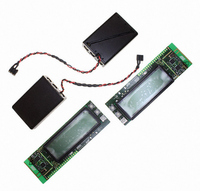
KIT DEMO FOR ATR2406/ATMEGA88
Manufacturer
Atmel
Series
Smart RFr
Type
Transceiver, ISMr
Datasheet
1.ATR2406-DEV-BOARD.pdf
(25 pages)
Specifications of ATR2406-DEV-KIT2
Frequency
2.4GHz
Wireless Frequency
2.4 GHz
Interface Type
SPI
Modulation
GFSK
Operating Voltage
2.9 V to 3.6 V
Operating Temperature Range
- 10 C to + 60 C
For Use With/related Products
ATR2406
Lead Free Status / RoHS Status
Contains lead / RoHS non-compliant


7.2
7.3
Note:
7.4
Note:
7.5
4779N–ISM–12/08
MSB
D15
MSB
D24
D15
0
1
0
RX Register Setting
Register Setting Without Clock Recovery
X values are not relevant and can be set to 0 or 1.
RX Register Setting with Internal Clock Recovery
X values are not relevant and can be set to 0 or 1.
PLL Settings
D14
D23
D14
1
0
0
D13
X
D22
D13
X
1
D12
X
There are two RX settings possible. For a data rate of 1152 kBits/s, an internal clock recovery
function is implemented.
Must be used for data rates below 1.152 Mbits/s.
Recommended for 1.152-Mbit/s data rate.
The output pin of the recovered clock is pin 6. The falling edge of the recovered clock signal
samples the data signal.
RC, MC and SC bits control the synthesizer frequency as shown in
12
Formula for calculating the frequency:
TX frequency: f
RX frequency: f
Table 7-3.
D21
D12
0
X
and
D11
Data bits
X
Table 7-5 on page
D20
D11
0
X
D10
PLL Settings of the Reference Counter Bit D7
X
ANT
ANT
D19
D10
= 864 kHz
= 864 kHz
0
X
D9
X
D7
0
1
12.
D18
D9
0
X
D8
0
Data bits
Data bits
(32
(32
D17
D8
0
0
RC (Reference Counter)
RC
D7
S
S
MC
MC
D16
RC
D7
0
+ S
+ S
D6
SC
SC
D6
MC
)
– 1)
MC
D5
D5
D4
D4
CLK Reference
10.368 MHz
13.824 MHz
Table
D3
D3
7-3,
SC
D2
D2
SC
Table 7-4 on page
ATR2406
D1
D1
LSB
LSB
D0
D0
11
Related parts for ATR2406-DEV-KIT2
Image
Part Number
Description
Manufacturer
Datasheet
Request
R

Part Number:
Description:
BOARD DEVELOPMENT FOR ATR2406
Manufacturer:
Atmel
Datasheet:

Part Number:
Description:
IC IF ISM TXRX 2.4GHZ 32QFN
Manufacturer:
Atmel
Datasheet:

Part Number:
Description:
BOARD DEV FOR ATR2406/ATMEGA88
Manufacturer:
Atmel
Datasheet:

Part Number:
Description:
Atr2406 Low-if 2.4-ghz Ism Transceiver
Manufacturer:
ATMEL Corporation
Datasheet:

Part Number:
Description:
RF Transceiver COM.ISM-SMART RF 2.4GHZ ISM TRX
Manufacturer:
Atmel
Datasheet:

Part Number:
Description:
Manufacturer:
Atmel
Datasheet:


Part Number:
Description:
LOW IF .4 GHZ ISM TRANSCEIVER
Manufacturer:
ATMEL [ATMEL Corporation]
Datasheet:

Part Number:
Description:
DEV KIT FOR AVR/AVR32
Manufacturer:
Atmel
Datasheet:
Part Number:
Description:
INTERVAL AND WIPE/WASH WIPER CONTROL IC WITH DELAY
Manufacturer:
ATMEL Corporation
Datasheet:
Part Number:
Description:
Low-Voltage Voice-Switched IC for Hands-Free Operation
Manufacturer:
ATMEL Corporation
Datasheet:
Part Number:
Description:
MONOLITHIC INTEGRATED FEATUREPHONE CIRCUIT
Manufacturer:
ATMEL Corporation
Datasheet:
Part Number:
Description:
AM-FM Receiver IC U4255BM-M
Manufacturer:
ATMEL Corporation
Datasheet:
Part Number:
Description:
Monolithic Integrated Feature Phone Circuit
Manufacturer:
ATMEL Corporation
Datasheet: