ATR2406-DEV-BOARD2 Atmel, ATR2406-DEV-BOARD2 Datasheet - Page 15
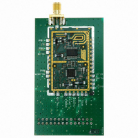
ATR2406-DEV-BOARD2
Manufacturer Part Number
ATR2406-DEV-BOARD2
Description
BOARD DEV FOR ATR2406/ATMEGA88
Manufacturer
Atmel
Series
Smart RFr
Type
Transceiver, ISMr
Datasheet
1.ATR2406-DEV-BOARD.pdf
(25 pages)
Specifications of ATR2406-DEV-BOARD2
Frequency
2.4GHz
Wireless Frequency
2.4 GHz
Interface Type
SPI
Modulation
GFSK
Operating Voltage
2.9 V to 3.6 V
Antenna
F-Antenna, SMA
Operating Temperature Range
- 10 C to + 60 C
For Use With/related Products
ATR2406, T7024
Lead Free Status / RoHS Status
Contains lead / RoHS non-compliant


7.10
4779N–ISM–12/08
Received Signal Strength Indication (RSSI)
Table 7-9.
The RSSI is given as an analog voltage at the RSSI pin. A typical plot of the RSSI value is
shown in
Figure 7-4.
Condition
C1
C2
C3
C4
C5
Figure
Description of the Conditions/States
Typical RSSI Value versus Input Power
7-4.
Description
Power down
ATR2406 is switched off and the supply current is lower than 1 µA.
Power up
ATR2406 is powered up by toggling PU_REG and PU_TRX to high.
PU_REG enables the external AUX regulator transistor including VCO regulator.
PU_TRX enables internal blocks like the PLL and the VCO.
Depending on the value of the external capacitors (for example, at the AUX
regulator, if one is used), it is necessary to wait at least 40 µs until the different
supply voltages have settled.
Programming
The internal register of the ATR2406 is programmed via the three-wire interface.
At TX, this is just the PLL (transmit channel) and the deviation (Gaussian filter).
At RX, this is just the PLL (receive channel) and, if the clock recovery is used, also
the bits to enable this option. At the start of the three-wire programming, the
enable signal is toggled from high to low to enable clocking the data into the
internal register. When the enable signal rises again to high, the programmed
data is latched. This is the time point at which the settling of the PLL starts. It is
necessary to wait the settling time of 200 µs so that the VCO frequency is stable.
The reference clock needs to be applied to ATR2406 for at least the time when the
PLL is in operation, which is the programming state (C3) and the active slot (C4,
C5). Out of the reference clock, several internal signals are also derived, for
example, the Gaussian filter circuitry and TX_DATA sampling.
This is the receive slot where the transmit burst is received and data as well as
recovered clock are available.
This is the active transmit slot. As soon as TX_DATA is applied to ATR2406, the
signal nOLE toggles to low which enables modulation in open-loop mode.
The preamble (1-0-1-0 pattern) should start being sent at the start of TX_ON.
2.0
0.0
2.5
0.5
1.0
1.5
-130
-110
-90
RF Level (dBm)
-70
-50
-30
-10
10
ATR2406
15
Related parts for ATR2406-DEV-BOARD2
Image
Part Number
Description
Manufacturer
Datasheet
Request
R

Part Number:
Description:
BOARD DEVELOPMENT FOR ATR2406
Manufacturer:
Atmel
Datasheet:

Part Number:
Description:
KIT DEMO FOR ATR2406/ATMEGA88
Manufacturer:
Atmel
Datasheet:

Part Number:
Description:
LOW IF .4 GHZ ISM TRANSCEIVER
Manufacturer:
ATMEL [ATMEL Corporation]
Datasheet:

Part Number:
Description:
IC IF ISM TXRX 2.4GHZ 32QFN
Manufacturer:
Atmel
Datasheet:

Part Number:
Description:
Atr2406 Low-if 2.4-ghz Ism Transceiver
Manufacturer:
ATMEL Corporation
Datasheet:

Part Number:
Description:
RF Transceiver COM.ISM-SMART RF 2.4GHZ ISM TRX
Manufacturer:
Atmel
Datasheet:

Part Number:
Description:
Manufacturer:
Atmel
Datasheet:


Part Number:
Description:
DEV KIT FOR AVR/AVR32
Manufacturer:
Atmel
Datasheet:
Part Number:
Description:
INTERVAL AND WIPE/WASH WIPER CONTROL IC WITH DELAY
Manufacturer:
ATMEL Corporation
Datasheet:
Part Number:
Description:
Low-Voltage Voice-Switched IC for Hands-Free Operation
Manufacturer:
ATMEL Corporation
Datasheet:
Part Number:
Description:
MONOLITHIC INTEGRATED FEATUREPHONE CIRCUIT
Manufacturer:
ATMEL Corporation
Datasheet:
Part Number:
Description:
AM-FM Receiver IC U4255BM-M
Manufacturer:
ATMEL Corporation
Datasheet:
Part Number:
Description:
Monolithic Integrated Feature Phone Circuit
Manufacturer:
ATMEL Corporation
Datasheet: