DM163027-5 Microchip Technology, DM163027-5 Datasheet - Page 32
DM163027-5
Manufacturer Part Number
DM163027-5
Description
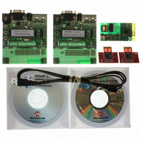
KIT DEMO PICDEM Z MRF24J40
Manufacturer
Microchip Technology
Series
PICDEM™ Zr
Type
802.15.4r
Datasheet
1.DM163027-5.pdf
(42 pages)
Specifications of DM163027-5
Frequency
2.4GHz
Wireless Frequency
2.4 GHz
Interface Type
RS-232
For Use With/related Products
MRF24J40MA
Lead Free Status / RoHS Status
Lead free / RoHS Compliant
Lead Free Status / RoHS Status
Lead free / RoHS Compliant, Lead free / RoHS Compliant


PICDEM Z Demonstration Kit User’s Guide
C.4
DS51524C-page 28
PCB LAYOUT
The PICDEM Z MRF24J40 2.4 GHz Daughter Card is fabricated as a four layer PCB.
The material is FR4 with signal traces in 0.5 oz copper. Figure C-4 through Figure C-9
show the individual layers from top to bottom. Figure C-10 shows the layer stack up.
The following guidelines are intended to aid users in high-frequency PCB layout
design. The printed circuit board is comprised of four basic FR4 layers: signal layout,
RF ground, power line routing and ground (see Figure C-3). The guidelines will explain
the requirements of these layers.
FIGURE C-3:
• It is important to keep the original PCB thickness since any change will affect
• The first layer width of a 50Ω characteristic impedance microstrip line is 12 mils.
• Avoid having microstrip lines longer than 2.5 cm, since that line might get very
• Except for the antenna layout, avoid sharp corners since they can act as an
• Digital lines by definition are prone to be very noisy when handling periodic
• A via filled ground patch underneath the IC transceiver is mandatory.
• A power supply must be distributed to each pin in a star topology and low-ESR
• Thorough decoupling on each power pin is beneficial for reducing in-band trans-
• Passive components (inductors) must be in the high-frequency category and the
antenna performance (see total thickness of dielectric) or microstrip lines
characteristic impedance.
close to a quarter wave length of the working frequency of the board which is
3.0 cm, and start behaving as an antenna.
antenna. Round corners will eliminate possible future EMI problems.
waveforms and fast clock/switching rates. Avoid laying out a RF signal close to
any digital lines.
capacitors must be placed at each pin for proper decoupling noise.
ceiver noise, particularly when this noise degrades performance. Usually, low
value caps (27-47 pF) combined with large value caps (100 nF) will cover a large
spectrum of frequency.
SRF (Self-Resonant Frequency) should be at least two times higher than the
operating frequency.
Note:
Care should be taken with all ground lines to prevent breakage.
FOUR BASIC COPPER FR4 LAYERS
Signal Layout, Thickness = 1.8 mils
Dielectric ε = 4.5, Thickness = 7 mils
RF Ground, Thickness = 1.2 mils
Dielectric ε = 4.5, Thickness = 19 mils
Power Line Routing, Thickness = 1.2 mils
Dielectric ε = 4.5, Thickness = 7 mils
Ground, Thickness = 1.8 mils
© 2008 Microchip Technology Inc.
Related parts for DM163027-5
Image
Part Number
Description
Manufacturer
Datasheet
Request
R

Part Number:
Description:
SERIES CONNECTION; 16 DIODES
Manufacturer:
Altech Corp.
Datasheet:

Part Number:
Description:
Manufacturer:
Microchip Technology Inc.
Datasheet:
Part Number:
Description:
Manufacturer:
Microchip Technology Inc.
Datasheet:
Part Number:
Description:
Manufacturer:
Microchip Technology Inc.
Datasheet:
Part Number:
Description:
Manufacturer:
Microchip Technology Inc.
Datasheet:
Part Number:
Description:
Manufacturer:
Microchip Technology Inc.
Datasheet:
Part Number:
Description:
Manufacturer:
Microchip Technology Inc.
Datasheet:
Part Number:
Description:
Manufacturer:
Microchip Technology Inc.
Datasheet:
Part Number:
Description:
Manufacturer:
Microchip Technology Inc.
Datasheet: