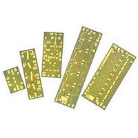
AMMC-6425-W50 Avago Technologies US Inc., AMMC-6425-W50 Datasheet - Page 2

AMMC-6425-W50
Manufacturer Part Number
AMMC-6425-W50
Description
IC MMIC 1W POWER AMP 18-28GHZ
Manufacturer
Avago Technologies US Inc.
Type
Power Amplifierr
Datasheet
1.AMMC-6425-W50.pdf
(7 pages)
Specifications of AMMC-6425-W50
Function
Amplifier
Supply Current
900mA
Supply Voltage Range
5V
Frequency Max
28GHz
Frequency Min
18GHz
Supply Voltage Max
7V
Gain
20dB
Number Of Channels
1
Frequency (max)
28GHz
Output Power
28.5@28000MHzdBm
Power Supply Requirement
Single
Single Supply Voltage (typ)
5V
Single Supply Voltage (max)
7V
Package Type
Chip
Dual Supply Voltage (min)
Not RequiredV
Dual Supply Voltage (typ)
Not RequiredV
Dual Supply Voltage (max)
Not RequiredV
Lead Free Status / RoHS Status
Lead free / RoHS Compliant
Lead Free Status / RoHS Status
Lead free / RoHS Compliant, Lead free / RoHS Compliant
Available stocks
Company
Part Number
Manufacturer
Quantity
Price
Part Number:
AMMC-6425-W50
Manufacturer:
AVAGO/安华高
Quantity:
20 000
AMMC-6425 DC Specifications/Physical Properties
Notes:
1. Ambient operational temperature T
2. Channel-to-backside Thermal Resistance (θ
AMMC-6425 RF Specifications
Notes:
3. Small/Large -signal data measured in wafer form T
4. 100% on-wafer RF test is done at frequency = 18, 23, and 28 GHz. Statistics based on 1500 part sample
5. Specifications are derived from measurements in a 50 Ω test environment. Aspects of the amplifier performance may be improved over a
Gain at 23 GHz
Typical distribution of Small Signal Gain and Output Power @P-1dB. Based on 1500 part sampled over several produc-
tion lots.
1. 17 17. 18 18. 19 19. 0 0. 1
Symbol
I
V
q
Symbol
Gain
P
P
OIP3
RLin
RLout
Isolation
dq
ch-b
-1dB
-3dB
LSL
g
at backside temperature (T
more narrow bandwidth by application of additional conjugate, linearity, or power matching.
Parameters and Test Conditions
Small-signal Gain
Output Power at 1dB Gain Compression
Output Power at 3dB Gain Compression
Third Order Intercept Point;
Df=100MHz; Pin=-20dBm
Input Return Loss
Output Return Loss
Min. Reverse Isolation
Parameters and Test Conditions
Drain Supply Current
(under any RF power drive and temperature)
(V
Gate Supply Operating Voltage
(I
Thermal Resistance
(Backside temperature, T
d(Q)
d
=5.0 V, V
= 900 (mA))
b
) = 25°C calculated from measured data.
g
set for I
[3, 4, 5]
[4]
[4]
A
[4]
=25°C unless otherwise noted.
[2]
(T
d
Typical)
A
= 25°C, V
b
ch-b
= 25°C)
P-1dB at 18 GHz
) = 10°C/W at T
LSL
A
= 25°C.
d
=5V, I
[1]
8
d(Q)=
channel
900 mA, Z
(T
Units
dB
dBm
dBm
dBm
dB
dB
dB
c
) = 107°C as measured using infrared microscopy. Thermal Resistance
Units
mA
V
°C/W
9
o
=50 Ω)
Minimum
16.5
27.5
Min.
-0.85
P-1dB at 28 GHz
Typical
18.5
28.5
30
38
-15
-14
-45
LSL
8
Typ.
900
-0.7
8.9
Maximum
9
Max.
1000
-0.55
Sigma
0.5
0.25
0.20
0.72
0.79
0.54
1.20


