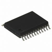
TA31275FNG Toshiba, TA31275FNG Datasheet - Page 5

TA31275FNG
Manufacturer Part Number
TA31275FNG
Description
IC RF/IF DETECTOR 450MHZ 24-SSOP
Manufacturer
Toshiba
Datasheet
1.TA31275EVKIT-315.pdf
(25 pages)
Specifications of TA31275FNG
Frequency
240MHz ~ 450MHz
Rf Type
AM, FM
Voltage - Supply
2.4 V ~ 5.5 V
Current - Supply
7.3mA
Package / Case
24-SSOP
Lead Free Status / RoHS Status
Lead free / RoHS Compliant
Accuracy
-
Input Range
-
Other names
TA31275FNGTR
Available stocks
Company
Part Number
Manufacturer
Quantity
Price
Company:
Part Number:
TA31275FNG
Manufacturer:
ETA
Quantity:
11 450
Part Number:
TA31275FNG
Manufacturer:
TOSHIBA/东芝
Quantity:
20 000
Functions
1. Waveform Shaper Circuit (comparator)
2. RSSI Function
3. V
4. Local Oscillator Circuit
5. RF Amp Current Adjustment
(pin 21) is converted to a voltage by the internal resistance. Thus, connecting external resistance R to pin
21 varies the gradient of the RSSI output as shown below. Note that due to the displacement of
temperature coefficients between external resistor R and the internal IC resistor IC resistor, the
temperature characteristic of the RSSI output may change. Also, the maximum RSSI value should be V
− 1 V or less, because AM doesn’t correct movement Filter AMP when voltage of RSSI high.
Also, use the same voltage supply source for GND1 (17 pin) and GND2 (8 pin) (or connect them).
level will become approximately 100dBµV.
using the ×8 circuit.
When R = 1 kΩ, the current dissipation is approximately 600 µA.
CC
The output data (pin 12) are inverted.
DC potential corresponding to the input level of IF IN (pin 6) is output to RSSI (pin 21). Output to RSSI
Use the same voltage supply for V
The local oscillator circuit is external-input-only. The device incorporates no transistor for oscillation.
Input to pin 1 at a level from 95 to 105dBµV.
Adjust the values of constants C107 and C108 shown in the application circuit diagram so that the input
By switching the Lo switch (LOBS), the frequency set by the external circuit can be used as-is without
The RF amp current dissipation can be regulated by varying resistor R as shown in the figure below.
Pin and GND Pin
Lo Switch (LOBS)
Local oscillation
status
Figure 1
21
×8 circuit in operation
CC
− Lo (2 pin) and V
H
Figure 3
RF DEC
14
5
CC1
(5 pin) and V
IF input level
×8 circuit halted/through pass
Figure 2
TA31275FN/ TA31275FNG
After R is
connected
L
CC2
(11 pin) (or connect them).
03-01-23
CC


