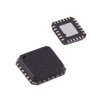
ADL5382ACPZ-R7 Analog Devices Inc, ADL5382ACPZ-R7 Datasheet - Page 13

ADL5382ACPZ-R7
Manufacturer Part Number
ADL5382ACPZ-R7
Description
IC DEMOD QUAD 700M2.7GHZ 24LFCSP
Manufacturer
Analog Devices Inc
Datasheet
1.ADL5382ACPZ-R7.pdf
(28 pages)
Specifications of ADL5382ACPZ-R7
Design Resources
Interfacing ADL5382 to AD9262 as an RF-to-Bits Solution (CN0062)
Function
Demodulator
Lo Frequency
700MHz ~ 2.7GHz
Rf Frequency
700MHz ~ 2.7GHz
P1db
14.5dBm
Gain
3.3dB
Noise Figure
17.6dB
Current - Supply
220mA
Voltage - Supply
4.75 V ~ 5.25 V
Package / Case
24-VFQFN, 24-CSP Exposed Pad
Frequency Range
700MHz To 2.7GHz
Rf Type
Quadrature
Supply Voltage Range
4.75V To 5.25V
Rf Ic Case Style
LFCSP
No. Of Pins
24
Operating Temperature Range
-40°C To +85°C
Lead Free Status / RoHS Status
Lead free / RoHS Compliant
Other names
ADL5382ACPZ-R7TR
Available stocks
Company
Part Number
Manufacturer
Quantity
Price
Company:
Part Number:
ADL5382ACPZ-R7
Manufacturer:
Analog Devices Inc
Quantity:
1 881
Part Number:
ADL5382ACPZ-R7
Manufacturer:
ADI/亚德诺
Quantity:
20 000
CIRCUIT DESCRIPTION
The ADL5382 can be divided into five sections: the local
oscillator (LO) interface, the RF voltage-to-current (V-to-I)
converter, the mixers, the differential emitter follower outputs,
and the bias circuit. A detailed block diagram of the device is
shown in Figure 39.
The LO interface generates two LO signals at 90° of phase
difference to drive two mixers in quadrature. RF signals are
converted into currents by the V-to-I converters that feed into
the two mixers. The differential I and Q outputs of the mixers
are buffered via emitter followers. Reference currents to each
section are generated by the bias circuit. A detailed description
of each section follows.
LO INTERFACE
The LO interface consists of a polyphase quadrature splitter
followed by a limiting amplifier. The LO input impedance is set
by the polyphase, which splits the LO signal into two differential
signals in quadrature. Each quadrature LO signal then passes
through a limiting amplifier that provides the mixer with a
limited drive signal. For optimal performance, the LO inputs
must be driven differentially.
RFIP
RFIN
Figure 39. Block Diagram
PHASE SPLITTER
QUADRATURE
POLYPHASE
BIAS
IHI
ILO
LOIP
LOIN
QHI
QLO
Rev. 0 | Page 13 of 28
V-TO-I CONVERTER
The differential RF input signal is applied to a resistively
degenerated common base stage, which converts the differential
input voltage to output currents. The output currents then
modulate the two half frequency LO carriers in the mixer stage.
MIXERS
The ADL5382 has two double-balanced mixers: one for the
in-phase channel (I channel) and one for the quadrature channel
(Q channel). These mixers are based on the Gilbert cell design
of four cross-connected transistors. The output currents from
the two mixers are summed together in the resistive loads that
then feed into the subsequent emitter follower buffers.
EMITTER FOLLOWER BUFFERS
The output emitter followers drive the differential I and Q
signals off-chip. The output impedance is set by on-chip 25 Ω
series resistors that yield a 50 Ω differential output impedance
for each baseband port. The fixed output impedance forms a
voltage divider with the load impedance that reduces the effective
gain. For example, a 500 Ω differential load has 1 dB lower
effective gain than a high (10 kΩ) differential load impedance.
BIAS CIRCUIT
A band gap reference circuit generates the proportional-to-
absolute temperature (PTAT) as well as temperature-independent
reference currents used by different sections. The mixer current
can be reduced via an external resistor between the BIAS pin
and ground. When the BIAS pin is open, the mixer runs at
maximum current and therefore the greatest dynamic range.
The mixer current can be reduced by placing a resistance to
ground; therefore, reducing overall power consumption, noise
figure, and IIP3. The effect on each of these parameters is
shown in Figure 10, Figure 13, and Figure 14.
ADL5382


