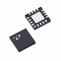
LT5516EUF Linear Technology, LT5516EUF Datasheet

LT5516EUF
Specifications of LT5516EUF
Available stocks
Related parts for LT5516EUF
LT5516EUF Summary of contents
Page 1
... IF filtering. Channel filtering can be performed directly at the outputs of the I and Q channels. These outputs can interface directly to channel- select filters (LPFs baseband amplifier. LT, LTC and LTM are registered trademarks of Linear Technology Corporation. All other trademarks are the property of their respective owners ...
Page 2
... Voltage Gain, Load Impedance = 1k – 40°C to 85° 8.2Ω 3.3Ω, P 2-Tone, –10dBm/Tone 8.2Ω ∆f = 200kHz R1 = 3.3Ω, P Input = –10dBm R1 = 8.2Ω 3.3Ω 8.2Ω (Note 4) (Note 4) Differential U W TOP VIEW ORDER PART NUMBER LT5516EUF – PART MARKING UF PACKAGE 5516 = 125° ...
Page 3
DC ELECTRICAL CHARACTERISTICS PARAMETER Supply Voltage Supply Current Shutdown Current Turn-On Time Turn-Off Time EN = High (On Low (Off) EN Input Current Output DC Offset Voltage + – + – ⏐ ⏐ ⏐ ⏐ – ...
Page 4
LT5516 W U TYPICAL PERFOR A CE CHARACTERISTICS (Test circuit optimized for 900MHz operation as shown in Figure 2) Supply Current vs Supply Voltage 160 R1 = 8.2Ω 85°C A 140 T = 25°C A 120 T = ...
Page 5
W U TYPICAL PERFOR A CE CHARACTERISTICS (Test circuit optimized for 900MHz operation as shown in Figure 2) I/Q Phase Mismatch vs RF Input Frequency – 40° 85°C A ...
Page 6
LT5516 W U TYPICAL PERFOR A CE CHARACTERISTICS (Test circuit optimized for 900MHz operation as shown in Figure 2) LO-RF Leakage vs LO Input Power – 25° 8.2Ω – ...
Page 7
CTIO S GND (Pins 1, 4): Ground Pin. + – (Pins 2, 3): Differential RF Input Pins. These pins are internally biased to 1.54V. They must be driven with a differential signal. ...
Page 8
LT5516 TEST CIRCUITS T1 LDB31900M20C-416 C17 100pF Figure 3. Topside of Evaluation Board 8 C21 C18 OPT OPT J3 J5 – OUT OUT C19 C20 OPT OPT ...
Page 9
U U APPLICATIO S I FOR ATIO The LT5516 is a direct I/Q demodulator targeting high linearity receiver applications, including wireless infra- structure. It consists amplifier, I/Q mixers, a quadrature LO carrier generator and bias circuitry. The ...
Page 10
LT5516 U U APPLICATIO S I FOR ATIO I-Channel and Q-Channel Outputs Each of the I-channel and Q-channel outputs is internally connected to V though a 60Ω resistor. The output dc CC bias voltage is V – 0.68V. The outputs ...
Page 11
... MOLD FLASH. MOLD FLASH, IF PRESENT, SHALL NOT EXCEED 0.15mm ON ANY SIDE Information furnished by Linear Technology Corporation is believed to be accurate and reliable. However, no responsibility is assumed for its use. Linear Technology Corporation makes no represen- tation that the interconnection of its circuits as described herein will not infringe on existing patent rights. ...
Page 12
... Supply, 40MHz to 500MHz IF, –4dB to 57dB Linear Power Gain 48dB Dynamic Range, Temperature Compensated, 2. Supply SC70 Package 36dB Dynamic Range, SC70 Package RF Output to 3GHz, 17dBm IIP3, Integrated LO Buffer DC-3GHz, 20dBm IIP3, Integrated LO Buffer www.linear.com ● 5516fa LT 0406 REV A • PRINTED IN USA © LINEAR TECHNOLOGY CORPORATION 2003 ...


