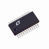
LT5502EGN Linear Technology, LT5502EGN Datasheet - Page 5

LT5502EGN
Manufacturer Part Number
LT5502EGN
Description
IC DEMOD IF QUADRATURE 24-SSOP
Manufacturer
Linear Technology
Datasheet
1.LT5502EGN.pdf
(12 pages)
Specifications of LT5502EGN
Function
Demodulator
Lo Frequency
140MHz ~ 800MHz
Rf Frequency
70MHz ~ 400MHz
Noise Figure
4dB
Current - Supply
32mA
Voltage - Supply
1.8 V ~ 5.25 V
Package / Case
24-SSOP
Lead Free Status / RoHS Status
Contains lead / RoHS non-compliant
Gain
-
P1db
-
Available stocks
Company
Part Number
Manufacturer
Quantity
Price
Part Number:
LT5502EGN
Manufacturer:
LINEAR/凌特
Quantity:
20 000
Company:
Part Number:
LT5502EGN#PBF
Manufacturer:
Linear Technology
Quantity:
135
Company:
Part Number:
LT5502EGN#PBF
Manufacturer:
LT
Quantity:
7 500
Part Number:
LT5502EGN#PBF
Manufacturer:
LINEAR/凌特
Quantity:
20 000
Part Number:
LT5502EGN#TRPBF
Manufacturer:
LINEAR/凌特
Quantity:
20 000
PI FU CTIO S
BLOCK DIAGRA
I
The DC bias voltage is V
shorted to ground.
I
The DC bias voltage is V
shorted to ground.
GND (Pins 3, 5, 8, 9, 14, 20, 21): Ground Pin.
V
should be decoupled using 1000pF and 0.1 F capacitors.
IF
V
IF
V
EN (Pin 10): Enable Pin. When the input voltage is higher
than 0.9V or up to V
When the input voltage is less than 0.7V or down to
ground, the circuit is turned off except the part of the
circuit associated with standby mode.
STBY (Pin 11): Standby Pin. When the input voltage is
higher than 0.9V or up to V
is turned on to bias the I/Q buffers to desired quiescent
OUT
OUT
CC
CC
CC
+
–
U
(Pin 6): Positive IF Input Pin. The DC bias voltage is
(Pin 7): Negative IF Input Pin. The DC bias voltage is
+
–
– 0.4V.
– 0.4V.
(Pins 4, 16, 17, 22): Power Supply Pin. This pin
(Pin 1): Positive Baseband Output Pin of I-Channel.
(Pin 2): Negative Baseband Input Pin of I-Channel.
U
CC
IF
U
IF
–
+
, the circuit is completely turned on.
CC
CC
6
7
– 1.16V. This pin should not be
– 1.16V. This pin should not be
W
CC
LIMITER
, the circuit of standby mode
1
IFt
12
+
RSSI
RSSI
15
IFt
13
–
LIMITER
2
BUFFERS
Q-MIXER
I-MIXER
LO
voltage. When the input voltage is less than 0.7V or down
to ground, it is turned off.
IFt
voltage is V
IFt
voltage is V
RSSI (Pin 15): RSSI Output Pin.
2XLO
signal’s frequency must be twice that of the desired
demodulator LO frequency. The DC bias voltage is V
0.4V.
2XLO
signal’s frequency must be twice that of the desired
demodulator LO frequency. The DC bias voltage is V
0.4V.
Q
Q-Channel. The DC bias voltage is V
should not be shorted to ground.
Q
Q-Channel. The DC bias voltage is V
should not be shorted to ground.
OUT
OUT
+
–
2XLO
(Pin 13): Interstage IF Negative Pin. The DC bias
(Pin 12): Interstage IF Positive Pin. The DC bias
–
+
–
+
19
DIVIDE 2
0 /90
(Pin 23): Negative Baseband Output Pin of the
(Pin 24): Positive Baseband Output Pin of the
+
(Pin 18): Negative Carrier Input Pin. The input-
(Pin 19): Positive Carrier Input Pin. The input-
2XLO
18
CC
CC
–
– 0.25V.
– 0.25V.
LPF
LPF
BIAS
1
1
10
EN
24
23
1
2
Q
Q
I
I
OUT
OUT
OUT
OUT
5502 BD
CC
CC
+
–
+
–
– 1.16V. This pin
– 1.16V. This pin
LT5502
CC
CC
5
–
–


