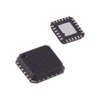
ADL5387ACPZ-R7 Analog Devices Inc, ADL5387ACPZ-R7 Datasheet - Page 18

ADL5387ACPZ-R7
Manufacturer Part Number
ADL5387ACPZ-R7
Description
IC QUADRATUR DEMOD 50MHZ 24LFCSP
Manufacturer
Analog Devices Inc
Datasheet
1.ADL5387ACPZ-R7.pdf
(28 pages)
Specifications of ADL5387ACPZ-R7
Function
Demodulator
Lo Frequency
100MHz ~ 2GHz
Rf Frequency
50MHz ~ 2GHz
P1db
12.8dBm
Gain
3.8dB
Noise Figure
16.5dB
Current - Supply
180mA
Voltage - Supply
4.75 V ~ 5.25 V
Package / Case
24-VFQFN, 24-CSP Exposed Pad
Frequency Range
50MHz To 2GHz
Rf Type
Quadrature
Supply Voltage Range
4.75V To 5.25V
Rf Ic Case Style
LFCSP
No. Of Pins
24
Operating Temperature Range
-40°C To +85°C
Frequency Max
2GHz
Lead Free Status / RoHS Status
Lead free / RoHS Compliant
Other names
ADL5387ACPZ-R7TR
Available stocks
Company
Part Number
Manufacturer
Quantity
Price
Company:
Part Number:
ADL5387ACPZ-R7
Manufacturer:
ADI
Quantity:
7 800
ADL5387
LOW IF IMAGE REJECTION
The image rejection ratio is the ratio of the intermediate
frequency (IF) signal level produced by the desired input
frequency to that produced by the image frequency. The image
rejection ratio is expressed in decibels. Appropriate image
rejection is critical because the image power can be much
higher than that of the desired signal, thereby plaguing the
down conversion process. Figure 54 illustrates the image
problem. If the upper sideband (lower sideband) is the desired
band, a 90° shift to the Q channel (I channel) cancels the image
at the lower sideband (upper sideband).
Figure 55 shows the excellent image rejection capabilities of the
ADL5387 for low IF applications, such as CDMA2000. The
ADL5387 exhibits image rejection greater than 45 dB over the
broad frequency range for an IF = 1.23 MHz.
–10
–20
–30
–40
–50
–60
–70
0
RF Input Frequency for a CDMA2000 Signal, IF = 1.23 MHz
50
250
450
ω
Figure 55. Image Rejection vs.
LSB
RF INPUT FREQUENCY (MHz)
650
ω
IF
ω
LO
850
ω
IF
ω
1050 1250 1450 1650 1850
USB
COS
SIN
ω
ω
LO
LO
t
t
Figure 54. Illustration of the Image Problem
Rev. 0 | Page 18 of 28
–
–
ω
ω
EXAMPLE BASEBAND INTERFACE
In most direct conversion receiver designs, it is desirable to
select a wanted carrier within a specified band. The desired
channel can be demodulated by tuning the LO to the appropriate
carrier frequency. If the desired RF band contains multiple
carriers of interest, the adjacent carriers would also be down
converted to a lower IF frequency. These adjacent carriers can
be problematic if they are large relative to the wanted carrier as
they can overdrive the baseband signal detection circuitry. As a
result, it is often necessary to insert a filter to provide sufficient
rejection of the adjacent carriers.
It is necessary to consider the overall source and load impedance
presented by the ADL5387 and ADC input to design the filter
network. The differential baseband output impedance of the
ADL5387 is 50 Ω. The ADL5387 is designed to drive a high
impedance ADC input. It may be desirable to terminate the
ADC input down to lower impedance by using a terminating
resistor, such as 500 Ω. The terminating resistor helps to better
define the input impedance at the ADC input. The order and
type of filter network depends on the desired high frequency
rejection required, pass-band ripple, and group delay. Filter
design tables provide outlines for various filter types and orders,
illustrating the normalized inductor and capacitor values for a
1 Hz cutoff frequency and 1 Ω load. After scaling the normalized
prototype element values by the actual desired cut-off frequency
and load impedance, the series reactance elements are halved to
realize the final balanced filter network component values.
IF
IF
0
0
+
+
ω
ω
IF
IF
–90°
+90°
0°
0°
0
0
+
+
ω
ω
IF
IF


