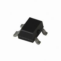
ADA-4543-TR1 Avago Technologies US Inc., ADA-4543-TR1 Datasheet - Page 2

ADA-4543-TR1
Manufacturer Part Number
ADA-4543-TR1
Description
IC AMP DARL BIPOL 2.5GHZ SOT-343
Manufacturer
Avago Technologies US Inc.
Datasheet
1.ADA-4543-TR1G.pdf
(10 pages)
Specifications of ADA-4543-TR1
Gain
15.1dB
Package / Case
SC-70-4, SC-82-4, SOT-323-4, SOT-343
Current - Supply
15mA
Frequency
0Hz ~ 2.5GHz
Noise Figure
3.7dB
P1db
1.9dBm
Rf Type
Cellular, PCS, WLL, WLAN
Test Frequency
900MHz
Voltage - Supply
3.1V ~ 3.8V
Peak Reflow Compatible (260 C)
No
Reel Quantity
3000
Noise Figure Typ
3.7dB
Power @ 1db Gain Compression, P1db
1.9
Leaded Process Compatible
No
Mounting Type
Through Hole
Lead Free Status / RoHS Status
Contains lead / RoHS non-compliant
Other names
516-1496-2
Available stocks
Company
Part Number
Manufacturer
Quantity
Price
Company:
Part Number:
ADA-4543-TR1G
Manufacturer:
AVAGO
Quantity:
7 500
Part Number:
ADA-4543-TR1G
Manufacturer:
AVAGO/安华高
Quantity:
20 000
2
ADA-4543 Absolute Maximum Ratings
P
P
T
T
ADA-4543 Electrical Specifications
T
Symbol
V
Gp
∆Gp
F
VSWR
VSWR
NF
P
OIP
DV/dT
Notes:
1. Typical value determined from a sample size of 500 parts from 3 wafers.
2. Measurement obtained using production test board described in the block diagram below.
3. I) 900 MHz OIP
Input
Block diagram of 900 MHz production test board used for V
Circuit losses have been de-embedded from actual measurements.
Symbol
I
θ
d
3dB
j
STG
d
diss
in max.
A
1dB
jc
II) 100 MHz OIP
= 25°C, Zo=50Ω, Pin = -25 dBm, I
3
in
out
Transmission
(0.5 dB loss)
50 Ohm
Parameter and Test Condition:
I
Device Voltage I
Power Gain (|S
Gain Flatness
3 dB Bandwidth
Input Voltage Standing Wave Ratio
Output Voltage Standing Wave Ratio
50Ω Noise Figure
Output Power at 1dB Gain Compression
Output 3
Device Voltage Temperature Coefficient
d
3
3
Parameter
Device Current
Total Power Dissipation
RF Input Power
Channel Temperature
Storage Temperature
Thermal Resistance
= 15 mA, Zo = 50Ω
test condition: F1 = 900 MHz, F2 = 905 MHz and Pin = -25 dBm per tone.
test condition: F1 = 100 MHz, F2 = 105 MHz and Pin = -25 dBm per tone.
rd
Order Intercept Point
21
d
= 15 mA
|
2
[3]
d
= 15 mA (unless specified otherwise)
[2]
[1]
DUT
Units
mA
mW
dBm
°C
°C
°C/W
d
, Gain, P
Frequency
100 MHz
900 MHz
100 to 900 MHz
0.1 to 2 GHz
0.1 to 6 GHz
0.1 to 6 GHz
100 MHz
900 MHz
100 MHz
900 MHz
100 MHz
900 MHz
1dB
, OIP
[1,2]
[1,2]
[1,2]
[3]
[1,2,3]
3
including Bias
Transmission
, and NF measurements.
(0.5 dB loss)
Absolute
Maximum
145
13
150
-65 to 150
152
40
50 Ohm
Units
V
dB
dB
GHz
dB
dBm
dBm
mV/°C
Output
Notes:
1. Operation of this device above any one of
2. Ground lead temperature is 25°C. Derate
3. Junction-to-case thermal resistance
Min.
3.1
13.5
these parameters may cause permanent
damage.
6.6 mW/°C for TL >128°C.
measured using 150°C Liquid Crystal
Measurement method.
Typ.
3.4
15.7
15.1
0.4
1.5
3.6
1.7:1
1.3:1
3.6
3.7
2.5
1.9
14.6
15.0
-5.6
Max.
3.8
16.5
Std. Dev.
0.16
0.18


