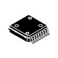
MHVIC910HNR2 Freescale Semiconductor, MHVIC910HNR2 Datasheet

MHVIC910HNR2
Specifications of MHVIC910HNR2
Available stocks
Related parts for MHVIC910HNR2
MHVIC910HNR2 Summary of contents
Page 1
... Technical Data 921 MHz - 960 MHz SiFET RF Integrated Power Amplifier The MHVIC910HNR2 integrated circuit is designed for GSM base stations, uses Freescale’s newest High Voltage (26 Volts) LDMOS IC technology, and contains a three - stage amplifier. Target applications include macrocell (driver function) and microcell base stations (final stage). The device PFP - 16 Power Flat Pack package which gives excellent thermal performances through a solderable backside contact ...
Page 2
... DQ3 Characteristic Frequency Range Output Power @ 1 dB Compression Point Power Gain @ P1dB Power Added Efficiency @ 1 dB Compression Point Input Return Loss @ P1dB Gain Flatness @ 40 dBm Variation ( +85° dBm) C MHVIC910HNR2 2 Rating 3 Symbol = 25°C matched Ω system, unless otherwise noted) Symbol 1dB G @ 1dB ...
Page 3
... AVX Chip Capacitor, ACCU−P (08053J330JBT) RF Device Data Freescale Semiconductor J1, J2 J3, J4 R1, R2, R3 PCB Figure 3. 921 - 960 MHz Demo Board Schematic OUTPUT Header (Break−away), HDR2X10STIMCSAFU SMA Connector 2052−1618−02 (Threaded) 100 Ω Chip Resistors (0402) Rogers 04350, 20 mils MHVIC910HNR2 3 ...
Page 4
... Freescale has begun the transition of marking Printed Circuit Boards (PCBs) with the Freescale Semiconductor signature/logo. PCBs may have either Motorola or Freescale markings during the transition period. These changes will have no impact on form, fit or function of the current product. Figure 4. 921 - 960 MHz Demo Board Component Layout MHVIC910HNR2 ...
Page 5
... I = 150 mA C DQ3 920 930 940 950 960 f, FREQUENCY (MHz) Figure 8. Power Gain versus Frequency out = +25° 120 mA C DQ3 T = +25° 150 mA C DQ3 f = 960 MHz 920 930 940 950 960 f, FREQUENCY (MHz out MHVIC910HNR2 +25°C 12 970 970 5 ...
Page 6
... Figure 13. Error Vector Magnitude versus SUPPLY VOLTAGE (VOLTS) DD Figure 15. Output Power versus Supply Voltage MHVIC910HNR2 6 TYPICAL CHARACTERISTICS −12 −14 − −18 − Vdc DD −22 950 960 970 910 Figure 12. Input Return Loss versus Frequency −50 −55 −60 −65 −70 2.0 W (RMS) −75 0.5 W (RMS) − ...
Page 7
... FREQUENCY (MHz) η P out Vdc 180 mA DQ total f = 880 MHz 0.5 1 1 INPUT POWER (mW) in η P out Vdc 160 mA DQ total f = 880 MHz 0.5 1 1 INPUT POWER (mW) in MHVIC910HNR2 0 −5 −10 −15 −20 −25 −30 −35 960 3 3.5 7 ...
Page 8
... MHVIC910HNR2 8 TYPICAL CHARACTERISTICS Vdc DQ total 880.0 MHz 880.1 MHz Two−Tone Measurement 100 kHz Tone Spacing 0 OUTPUT POWER (WATTS) PEP out Figure 23. Intermodulation Distortion versus Output Power = 140 mA 160 mA 170 mA 180 mA 10 ...
Page 9
... Z = Test circuit impedance as measured load from drain to ground. Output Device Matching Under Test Network Z load RF Device Data Freescale Semiconductor Figure 24. Series Equivalent Load Impedance f = 1000 MHz = 10 Ω load f = 900 MHz MHVIC910HNR2 9 ...
Page 10
... MHVIC910HNR2 10 NOTES RF Device Data Freescale Semiconductor ...
Page 11
... A1 0.025 0.100 A2 1.950 2.100 S D 6.950 7.100 D1 4.372 5.180 E 8.850 9.150 E1 6.950 7.100 E2 4.372 5.180 L 0.466 0.720 L1 0.250 BSC b 0.300 0.432 b1 0.300 0.375 c 0.180 0.279 c1 0.180 0.230 e 0.800 BSC h −−− 0.600 aaa 0.200 bbb 0.200 ccc 0.100 MHVIC910HNR2 11 ...
Page 12
... RoHS- compliant and/or non - Pb- free counterparts. For further information, see http://www.freescale.com or contact your Freescale sales representative. For information on Freescale’s Environmental Products program http://www.freescale.com/epp. MHVIC910HNR2 Document Number: MHVIC910HNR2 Rev. 9, 5/2006 12 RoHS-compliant and/or Pb- free versions of Freescale products have the functionality and electrical characteristics of their non-RoHS-compliant and/or non-Pb- free counterparts ...


